

Table of Contents
ToggleTo implement the design of certain functionalities on the PCB board, PCB design is based on the circuit schematic diagram. The layout design, exterior connection layout, optimal layout of internal electronic components, and other considerations should all be considered while designing a PCB. PCB design is responsible for standardizing design processes, increasing production efficiency, and improving the quality of electrical devices.
For PCB design, the following information is required:
A schematic diagram is a complete electronic document format that can be used to build the correct netlist and provide the layout and functionality that the PCB requires.
Mechanical size: offers many physical information to the PCB, such as the precise location and direction of electronic devices.
Device packaging: for PCB circuit boards, includes device packaging libraries, packaging methods, and electronic material specifications.
Specific signal requirements, impedance, and other PCB design information are provided in the wiring guide.
Here are a few examples of PCB design software:
1.protel, protel 99se, protel DXP, Altium Protel, Protel 99se, Protel DXP, Protel DXP, Protel DX
2.SPB software from Cadence
3.BORDSTATIONGoing and EE
4.EAGLE design
Here are the 10 steps of creating a printed circuit board, from the original designs to the final files:
1. Gain a thorough understanding of the electrical parameters.
Before beginning a PCB design, you need be familiar with and understand the system’s electrical parameters, which include:
Maximums at the moment
Voltages
Types of signals
Limitations in capacitance
The characteristics of impedance
Considerations to protect yourself
Types of circuit components and connectors, as well as their locations
Schematic and detailed list of net wires
2. Creating the blueprint.
Creating a schematic, which refers to the design of the board’s purpose and function at the electrical level, is always one of the initial tasks. It’s still not a mechanical representation at this stage.
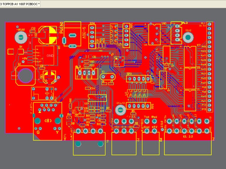
3. Create your PCB layout using a schematic capture program.
The ideal PCB provider will collaborate with principal engineers to create a schematic using a software platform like Mentor PADS®, Allegro, or Altium that demonstrates how your board will work and where the components will be put. After you finish your schematic, the mechanical engineer will load it into the gadget and assess how it will fit.
4. Create a PCB stackup.
Because of impedance, which relates to how much and how rapidly electricity may go along a trace, this is vital to address early in the PCB design stage. The stackup affects the mechanical engineer’s ability to design and fit the PCB into the device.
5. Establish design guidelines and specifications.
The IPC, which is the industry association for PCB and electronics manufacturing, sets the standards and approval criteria for this phase. These specifications cover all you need to know about PCB manufacture. A useful advice is to use a PCB layout company that is well-versed in IPC standards. This will help you prevent big changes and project delays.
6. Arrange your elements.
When it comes to component placement, the customer and PCB vendor will often debate design and layout parameters. Standards may state, for example, that certain components should not be placed near others because they induce electrical noise in the circuit. Every component (in most cases, connections) will have data sheets from the PCB vendor, which will be inserted in the mechanical layout and given to the customer for approval.
7. Drill holes in the board.
The components and a connection drive this step. About half of the flex circuits on the market are double-sided, meaning they link to the bottom layer’s drill hole.
8. Connect the wires.
You’re ready to route the traces, which entails linking portions of the path, after you’ve put the components and drilled holes.
9. Fill in the blanks with labels and identifiers.
Add any labels, IDs, markers, or reference designators to the layout at this point. Reference designators are useful for indicating the location of specific components on the board.
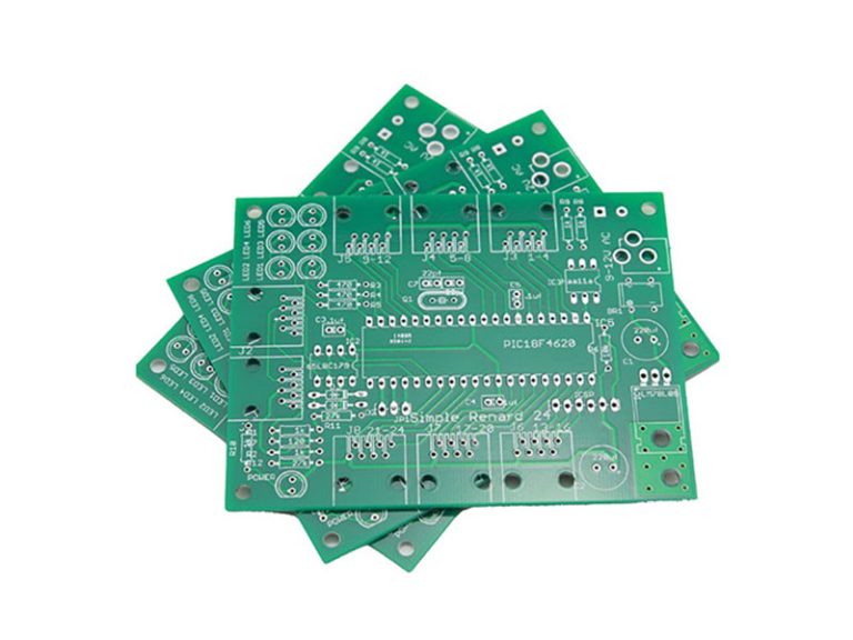
10. Create design and layout files.
The layout process comes to a close with this stage. These files include all of the information about your printed circuit board, and once they’ve been created, your PCB is ready to be fabricated, manufactured, and assembled.

-768x513.jpg)

-768x576.jpg)
