

DIP PCB Assembly
Why Choose LHD
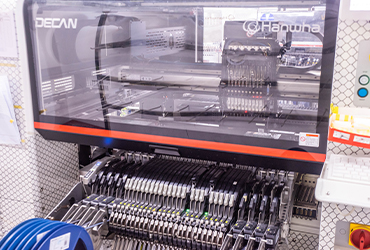
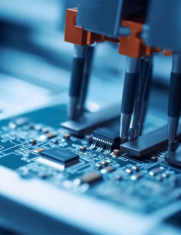
The latest equipment and technology are used for DIP assembly to ensure higher production efficiency and better welding quality.
Provide personalized services based on customers’ specific needs, including but not limited to the use of special materials, customized design improvements and special testing requirements.
Whether it is small batches or large-scale production, your company can respond flexibly to meet the needs of different customers.

Offer competitive prices without sacrificing product quality by optimizing production processes and bulk purchasing.

Provide comprehensive customer support, including project management, technical consulting and after-sales service to ensure customer satisfaction.
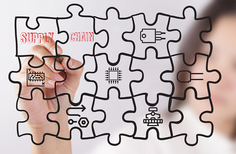
Have a stable and efficient supply chain management system to ensure timely delivery and high quality of materials.
DIP PCB assembly process services
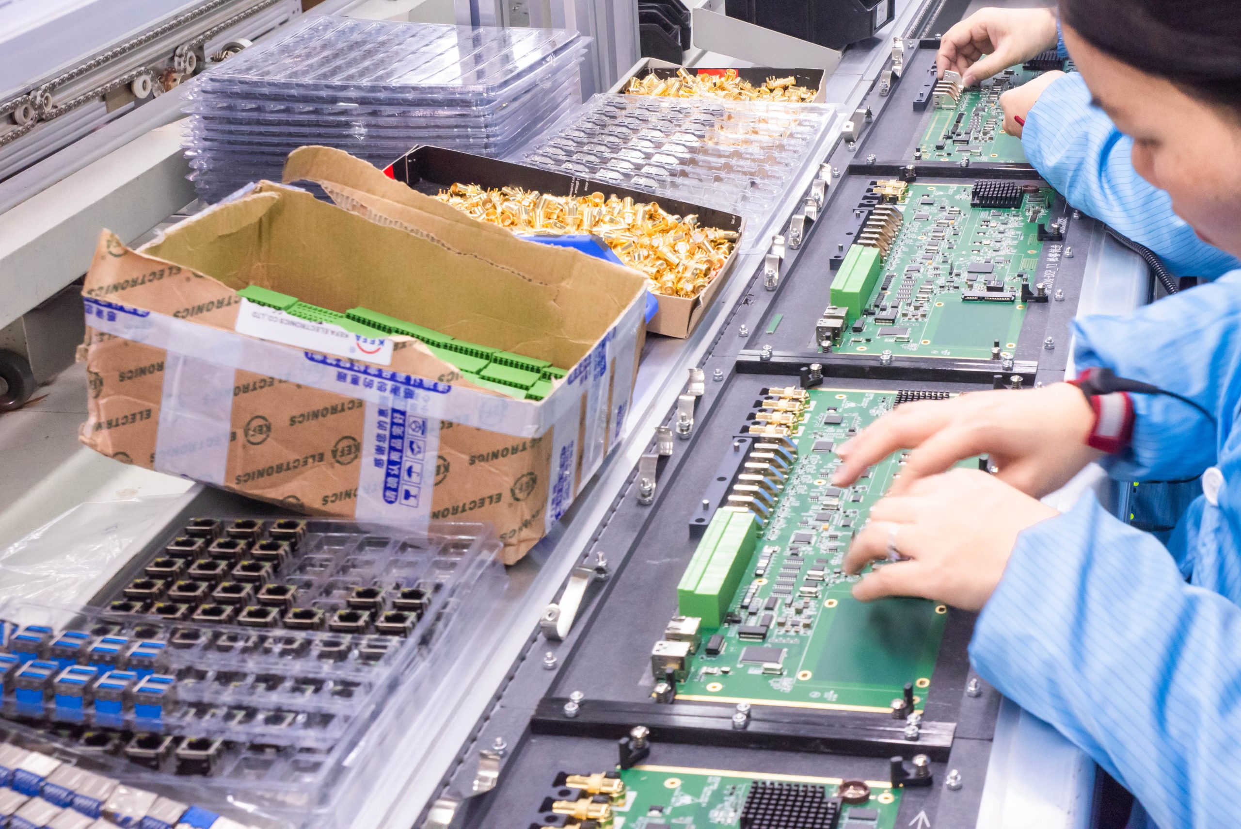
Component preparation:
Prepare the required electronic components and PCB boards according to customer needs and design drawings.
Manual/machine insertion
According to the component type and design requirements, components are inserted into the corresponding holes of the PCB board through manual or automatic machines.
Wave soldering/hand soldering
Use wave soldering techniques or hand soldering to secure components and ensure the reliability of electrical connections.
Inspection and Testing
Ensure all components are installed correctly and have no soldering defects through visual inspection and electrical testing.
Cleaning and Packaging
Clean the PCB board to remove the residue generated during the soldering process, and then carry out final packaging.
How I can help you be happier
— 01
AOI
Automated Optical Inspection uses a high-resolution camera to scan soldered components to check component placement and the quality of solder joints. AOI can quickly detect welding defects, component misalignments, missing parts and wrong polarity.
— 02
X-Ray Inspection
For parts where the welding quality is difficult to directly observe from the outside, such as the solder joints under the pins, X-ray inspection can be used for internal inspection. X-rays can reveal hidden defects under solder joints, such as cold welds and short circuits.
— 03
Functional Testing
Functional testing is to verify the performance of the PCB by simulating its working conditions in actual applications. This includes testing the power supply, signal input and output, and other functionality of the PCB circuit to ensure that the product is working properly according to specifications.
— 04
Electrical Testing
Automated Optical Inspection uses a high-resolution camera to scan soldered components to check component placement and the quality of solder joints. AOI can quickly detect welding defects, component misalignments, missing parts and wrong polarity.
— 05
Non-Destructive Testing
For parts where the welding quality is difficult to directly observe from the outside, such as the solder joints under the pins, X-ray inspection can be used for internal inspection. X-rays can reveal hidden defects under solder joints, such as cold welds and short circuits.
— 06
Aging Test
Functional testing is to verify the performance of the PCB by simulating its working conditions in actual applications. This includes testing the power supply, signal input and output, and other functionality of the PCB circuit to ensure that the product is working properly according to specifications.
