Multilayer PCB
What Is Multilayer PCB
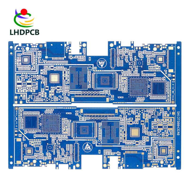
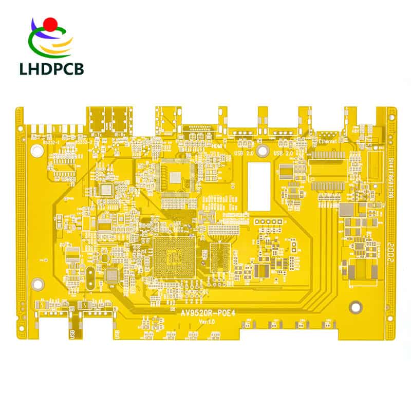
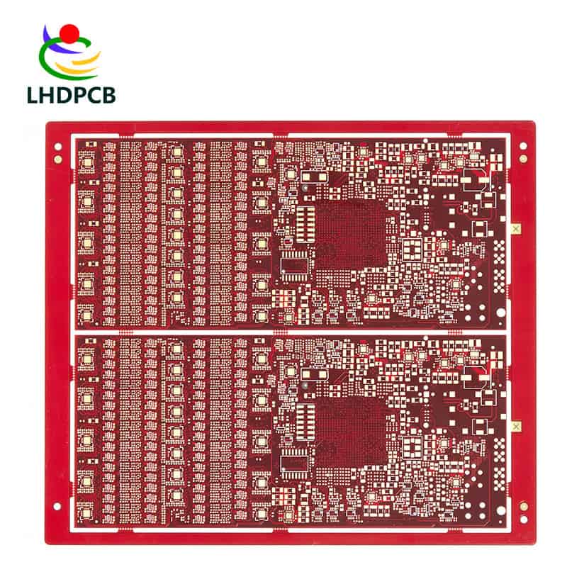
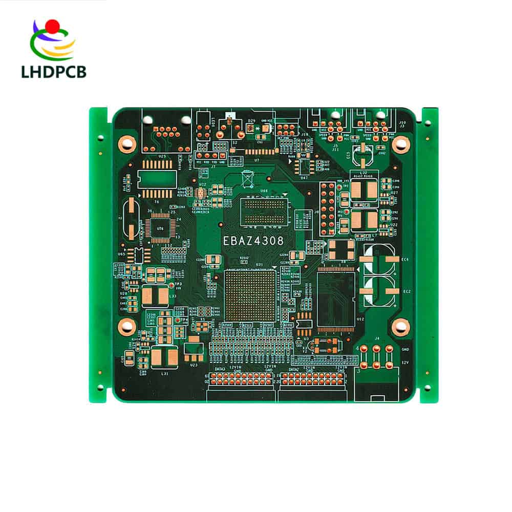
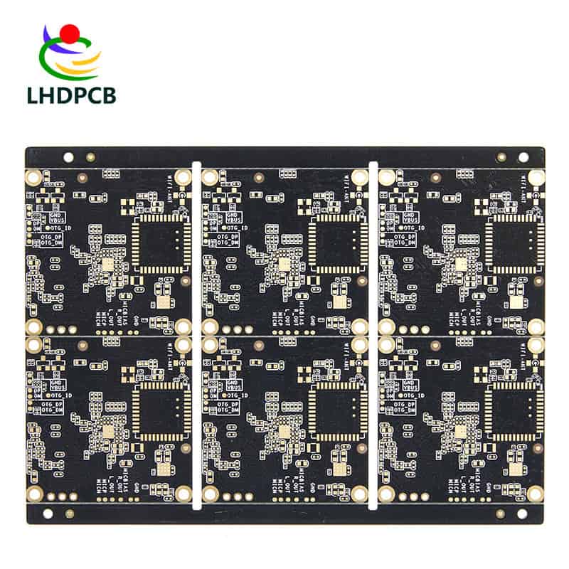
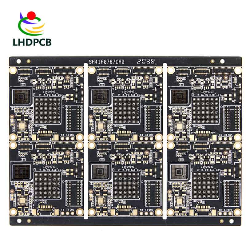
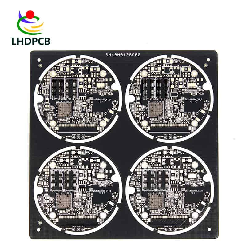
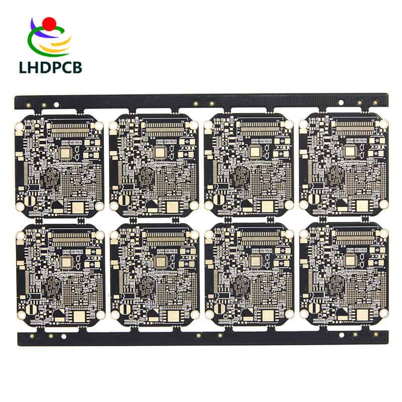
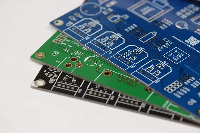
Multilayer PCB board refers to the multilayer board with more single panel or double panel wiring board. A printed circuit board with a double-sided inner layer, two single-sided outer layer or two double-sided inner layer, two single-sided outer layer, alternating together through the positioning system and insulating binder materials, and the conductive graphics are interconnected according to the design requirements of the printed circuit board becomes a four-layer, eight-layer, twelve layer, twenty layer printed circuit board, also known as high multilayer printed circuit board.
Why Choose LHD
With 20 years of history, we have accumulated rich experience in PCBA production and manufacturing, and have a deep understanding of industry development trends and customer needs.
01.
Advanced Manufacturing Technology
We use the most advanced manufacturing technology and equipment to ensure the high precision and quality of our PCBs.
02.
Experienced Team
A team with extensive expertise in the design and manufacturing of complex multi-layer PCBs.
03.
Customized Solutions
Provide customized designs and services according to specific customer needs.
04.
Strict Quality Control
From raw materials to final products, we implement strict quality control processes to ensure product reliability and consistency.
05.
Superior Customer Service
We provide comprehensive customer support and technical consultation to ensure customer satisfaction.
06.
Competitive Pricing
We have a very complete internal supply chain for raw materials and manufacturing processes, which enables us to better control costs and quality, and provide customers with competitive pricing.
What are the characteristics of common multilayer PCB?
The biggest difference between PCB multilayer board and single panel and double panel is that the internal power layer (to maintain the internal power layer) and ground layer are added, and the power and ground network are mainly routed on the power layer. However, the multilayer board wiring is mainly based on the top and bottom layers, supplemented by the middle wiring layer. Therefore, the design method of multilayer board is basically the same as that of double panel, and the key lies in how to optimize the wiring of the internal electrical layer.
- Thin type multi (high) layer
- Diversification of multilayer board structure
- Thin substrate for high-performance thin copper boxes
- High flatness and surface coating technology
- Flexible multilayer board and rigid flexible multilayer board
20 years of history
As the core component of modern electronic technology, high layer PCB is of great significance in the fields of communication, industrial control and consumer electronics. With the rapid development of 5G, the Internet of Things, artificial intelligence and other technologies, high-layer PCBS are promoting the digital transformation and upgrading of all walks of life.
Areas of Application
- Consumer Electronics
- Communication Devices
- Medical Equipment
- Military and Aerospace
- Industrial Control Systems
- Automotive
LHD Multilayer PCB Capability Overview
| Processing layers | 3-50 layers |
|---|---|
| Finished board thickness (thinnest - thickest) | 0.008″ ~ 0.24″ (0.20mm ~ 6.0mm) |
| Minimum Hole Diameter | 6mil (0.15mm) |
| Minimum line width/spacing | 3-4 mil (0.076-0.10mm) |
| Maximum board size | Multilayer 22″x 25″ (550mm x 640mm) |
| Impedance control | ± 10% |
| Surface treatment process | oxidation resistant OSP, tin spraying, electric nickel/gold, chemical nickel/gold, lead-free tin spraying, gold finger, immersion silver, immersion tin, thick nickel/gold. |
| Processing materials | FR4, high TG (TG150, TG170), halogen-free boards, high-frequency boards (Rogers, Teflon, Taconic), polytetrafluoroethylene (F4B, F4BK), copper-based, iron-based, ceramic substrates. |
Related Products