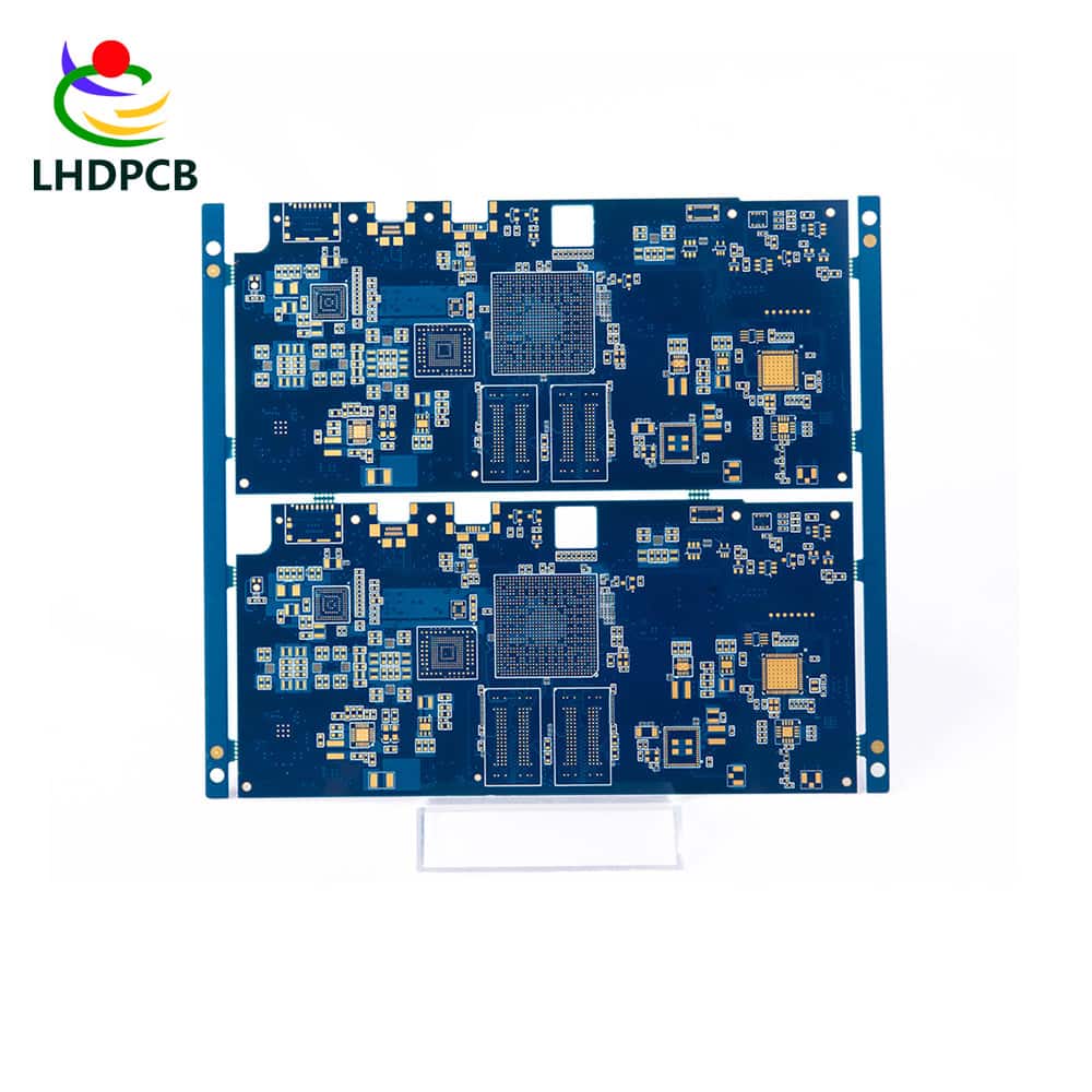
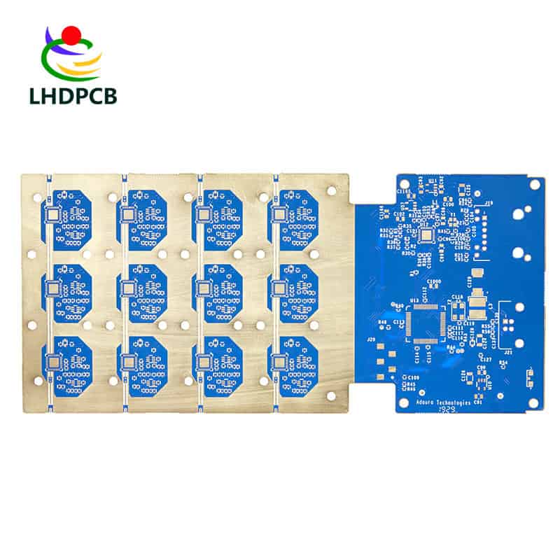
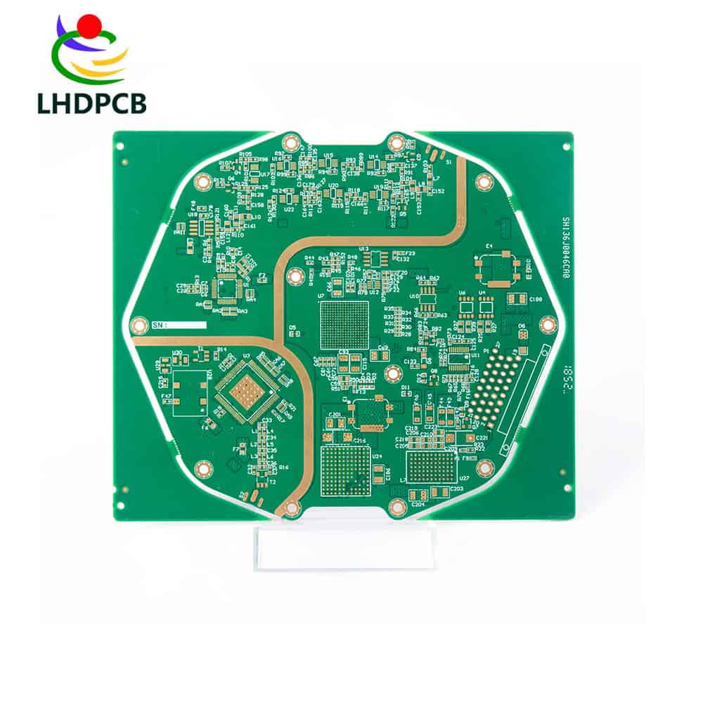
High Frequency PCB
What is a high frequency PCB
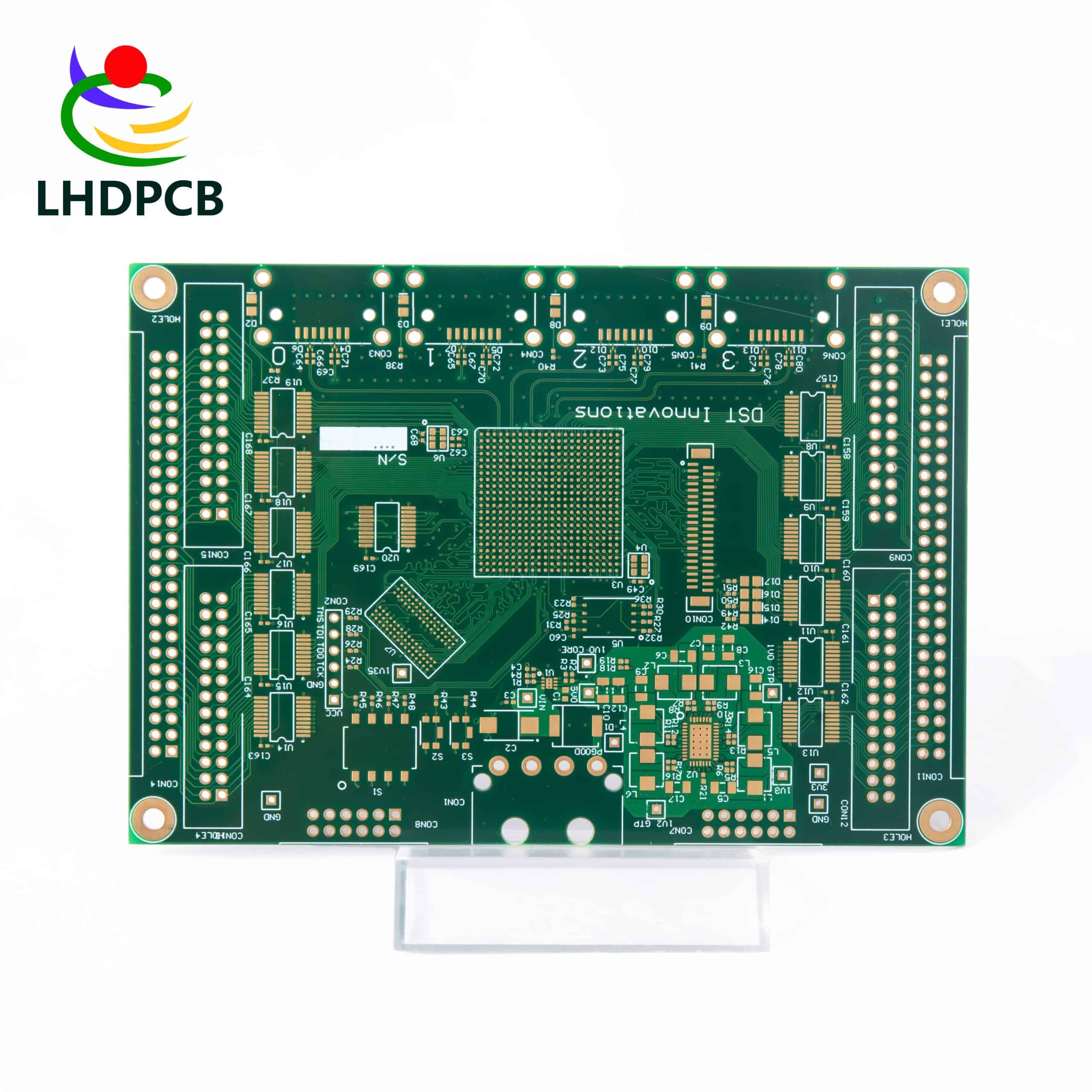
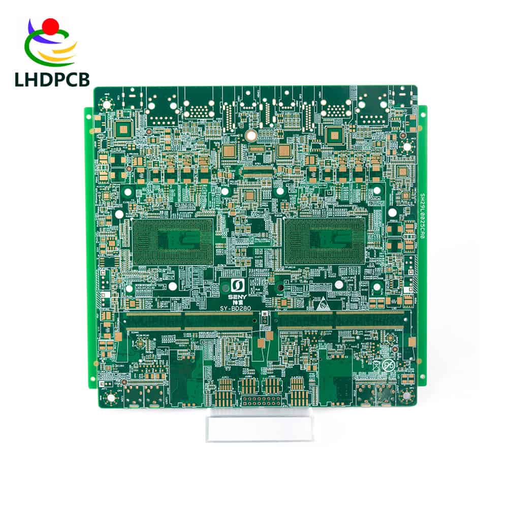
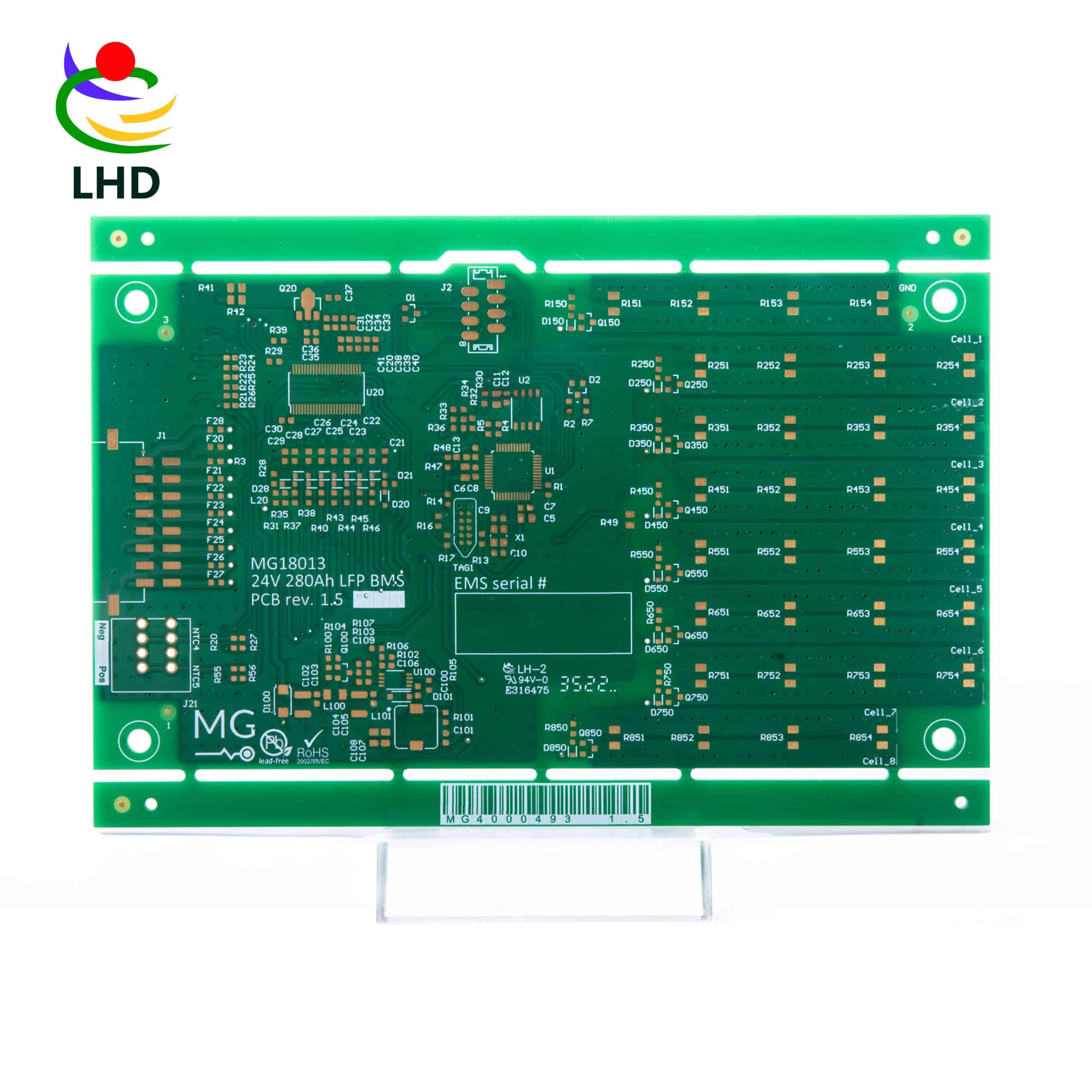
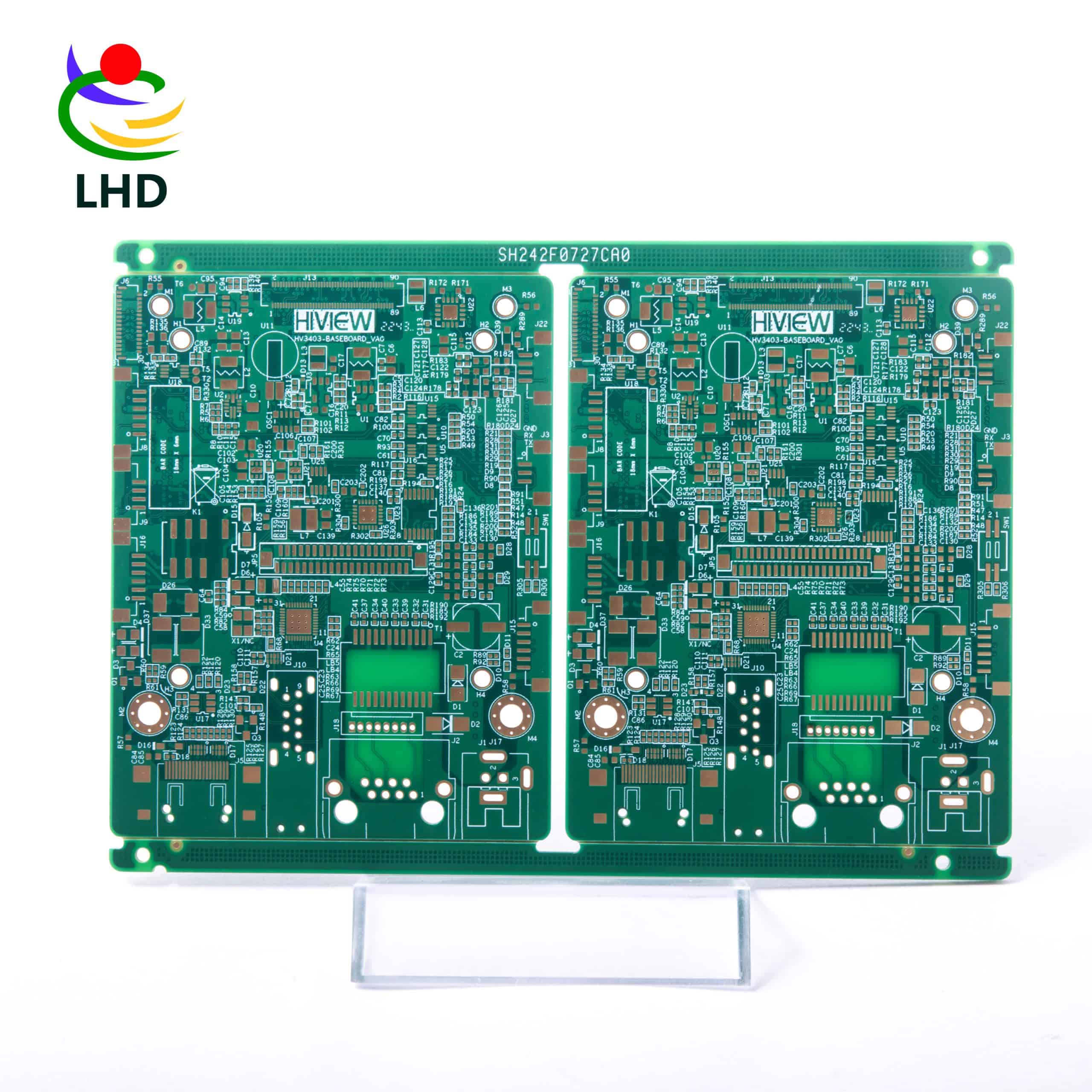
High-frequency PCB board refers to a special circuit board with a high electromagnetic frequency, used for PCB in the field of high frequency (frequency greater than 300MHZ or wavelength less than 1 meter) and microwave (frequency greater than 3GHZ or wavelength less than 0.1 meters), the key point to achieve high frequency and high speed is the properties of raw materials, that is, the characteristic parameters of raw materials. The main material of high-speed PCB board is high-frequency high-speed copper-clad plate, and its core requirement is to have low dielectric constant (Dk) and low dielectric loss factor (Df). In addition to ensuring lower Dk and Df, the consistency of Dk parameters is also one of the important factors to measure the quality of high-speed high-frequency PCB boards. In addition, there is an important parameter is the impedance characteristics of the PCB board and some other physical characteristics.
The dielectric constant (DK) of the substrate must be small and stable, generally speaking, the smaller the better, the signal transmission rate is inversely proportional to the square root of the dielectric of the material, and the high dielectric constant is easy to cause signal transmission delay.
The dielectric loss (DF) of the substrate material must be small, which mainly affects the quality of signal transmission, and the smaller the dielectric loss, the smaller the signal loss.
The impedance of the high-frequency high-speed PCB board – in fact, refers to the resistance and resistance parameters, impedance control is the most basic principle of our high-speed design, because the PCB line should consider the installation of electronic components, electrical conductivity and signal transmission performance after insertion, so the impedance is inevitably required to be as low as possible.
The water absorption of the substrate of the high-frequency high-speed PCB board should be low, and the high water absorption will cause the dielectric constant and medium loss when it is damp.
Characteristics of high frequency PCB
Field of application.
This circuit board is mainly used in fields that need to process high frequency or microwave signals, such as communication systems, automotive ADAS systems, satellite communication systems, radio systems, etc.
Technical requirements.
High frequency boards have very high requirements for physical properties, accuracy and technical parameters.
Material properties.
High frequency plate usually uses heat resistance, chemical corrosion resistance, impact resistance and good stripping performance of materials, such as Rogers, Tieflong, Sheng Yi, Taiwan light table, Yao Wang Ling, Taikangli and so on.
The manufacturing process.
The high-frequency plate may be produced on the microwave substrate copper-clad plate, using the manufacturing method of the ordinary rigid circuit board, combined with some special processes or special treatment methods.
Signal transmission.
High frequency plate can control the high precision and low loss of signal transmission, so it is widely used in modern communications, military electronics, aerospace and other fields.
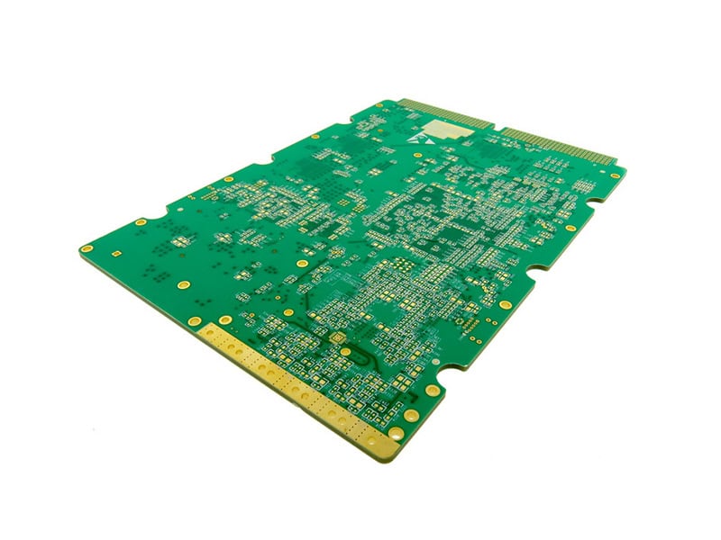
What are the materials used to make high frequency PCB board?
The performance of the high-frequency board in wireless or other high-frequency applications depends on the building material. For many applications, the use of laminated FR4 materials can improve dielectric properties. When manufacturing high-frequency PCB boards, the commonly used plates are Rogers /Rogers, Taikonick /Taconic, Isola (Isona), F4B (Teflon), TP-2, FR4, Panasonic, Taiyao and other plates.
Advantages of high frequency PCB
Good efficiency;
Fast working speed;
Applicability;
Strong tolerance, strong anti-interference ability

Low signal loss
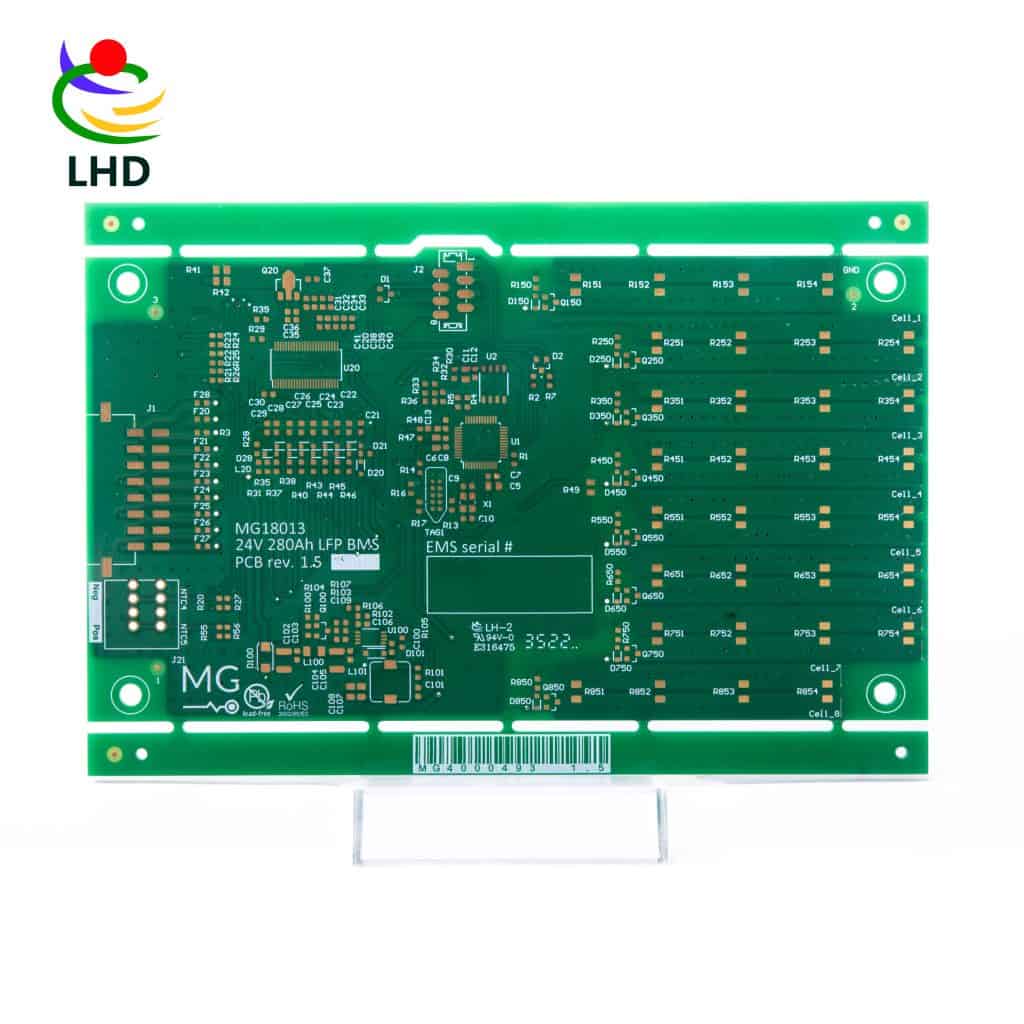
High signal integrity

Thermal management

Resistant to environmental impacts
Why Choose Us
Specialized knowledge and experience
we have rich experience in HF PCB design and manufacturing.
Advanced Manufacturing Technology
We use the most advanced equipment and technology to ensure the quality of our HF PCBs.
High-quality materials
We select high-quality HF materials to ensure optimal performance.
Customized design and service
Provide customized design and service according to customer's specific needs.
Strict Quality Control
Ensure that each PCB meets strict quality standards.

Areas of Application
- Communication Systems
- RF Applications
- Data Centers
- Medical Devices
- Aerospace
- Automotive Radar Systems
High frequency PCB Specification at LHD Technology
| Processing layers | 1-28 layers |
|---|---|
| Finished board thickness (thinnest - thickest) | 0.008″ ~ 0.24″ (0.20mm ~ 6.0mm) |
| Minimum Hole Diameter | 6mil (0.15mm) |
| Minimum line width/spacing | 3-4 mil (0.076-0.10mm) |
| Maximum board size | Single and double layer 22″x 43″ (550 x 1100mm) Multilayer 22″x 25″ (550mm x 640mm) |
| Impedance control | ± 10% |
| Surface treatment process | oxidation resistant OSP, tin spraying, electric nickel/gold, chemical nickel/gold, lead-free tin spraying, gold finger, immersion silver, immersion tin, thick nickel/gold. |
| Processing materials | FR4, high TG (TG150, TG170), halogen-free sheet, high-frequency sheet (Rogers, Teflon, Taconic). |
Related Products
