


01
Design and Output
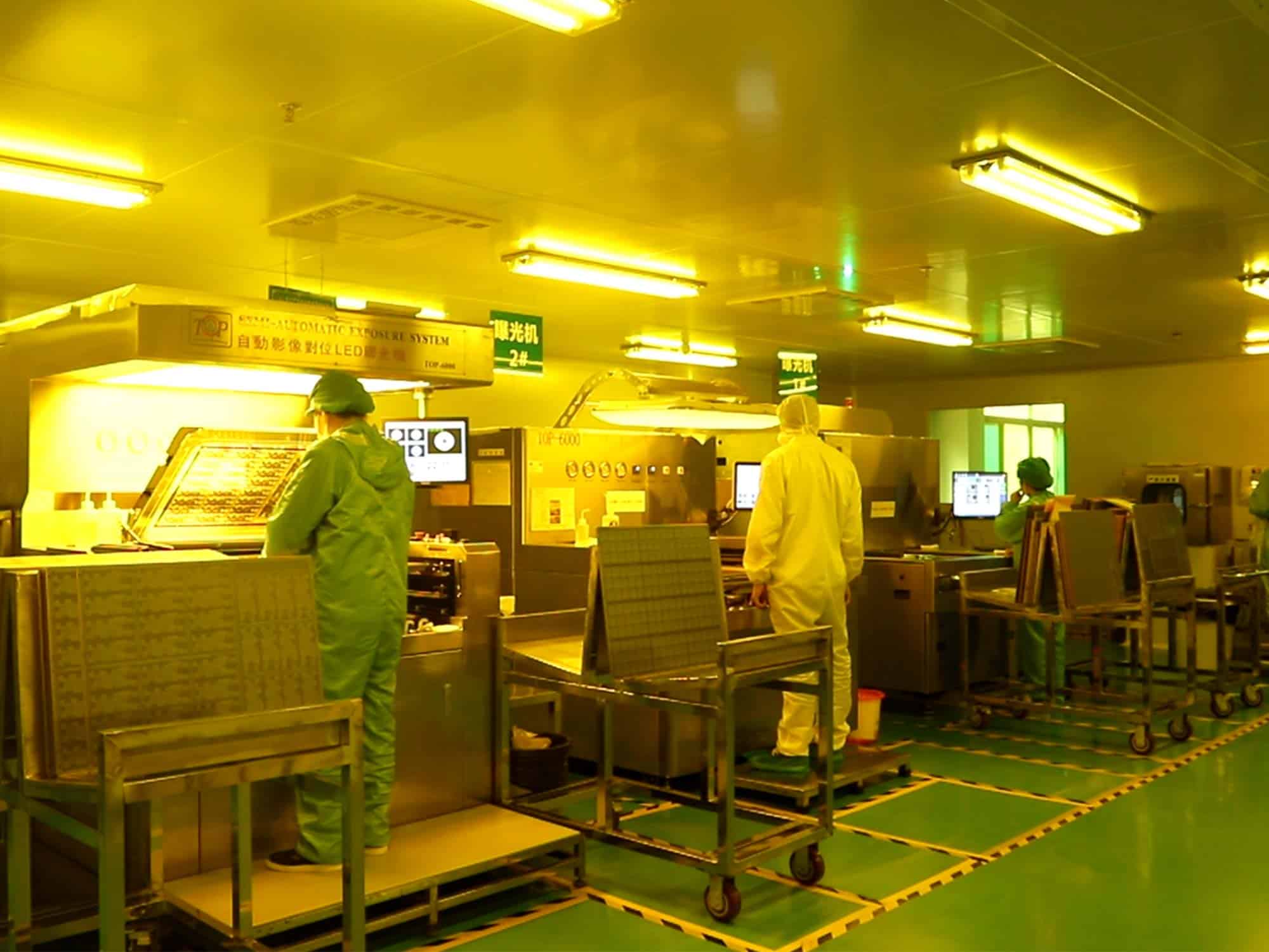
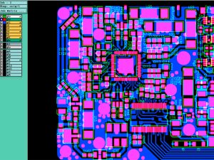
 -Design: Use professional design software (LHD PCB supports various design software such as Altium Designer, Eagle, KiCAD, PADS, Cadence Allegro, Protel, Proteus, EasyEDA, etc.) to design PCB layout and circuit diagrams. When designing, factors such as component layout, signal integrity, and power layer design need to be considered. After completion, it is recommended to use the software’s built-in DRC analysis function to analyze whether the design is reasonable and correct.
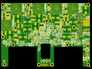
-Output: After the design is completed, output Gerber files and NC Drill files (LHD PCB supports various forms of file production PCB, such as Gerber 274&274X, ODB, tgz, DXF, DWG, etc.). These files provide all the necessary information for manufacturing PCBs, including the layout size, drilling hole positions, and sizes of copper wires and solder pads.
02
DFM Analysis
-LHD PCB provides free DFM analysis: PCB DFM analysis is an important step in PCB manufacturing, and DFM stands for “Design for Manufacturability”. DFM analysis aims to evaluate the manufacturability of PCB design and provide suggestions for improving the design to make it easier to manufacture, assemble, and test. This helps to avoid problems during the manufacturing process, improve the quality and production efficiency of PCBs. (See more DFM analysis )
03
Preparation of Production Materials
 -Selection of substrate material: The commonly used substrate material is FR-4, a glass fiber reinforced epoxy resin material with good insulation and mechanical strength. LHD PCB supports the production of various PCB boards, such as CEM1, CEM3, Fr1, FR-2, Fr4, Aluminum Based PCB, Metal Core PCB, Flex PCB and Rigid-Flex PCB, and High Frequency PCB (PTFE). In addition to the common types of boards mentioned above, there are also many special materials for specific purposes, such as ceramic substrates, polyimide (PI) boards, etc.
-Cutting substrate: Cut the large-sized board provided by the material factory into small boards that meet the required production line dimensions for subsequent processing.
04
Inner Circuit Production (For multi-layer PCB boards)
 -Inner layer graphic transfer: Print the copper sheets and circuit patterns from the Gerber files used in production onto the copper foil of the inner layer core board using photoresist transfer technology.
-Etching circuit: By using dry film and chemical etching, unnecessary copper skin parts are removed, leaving the customer with the required circuit and solder pads.
05
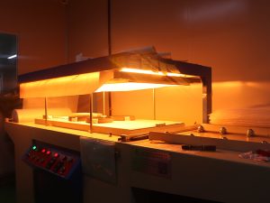
Lamination (Used for multi-layer PCB boards)
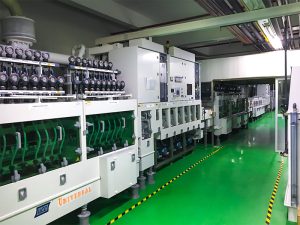
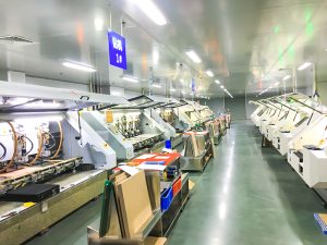
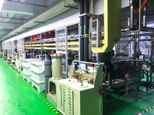
 The LHD PCB factory has multiple hot fully active laminating machines that can quickly and stably complete the lamination production of various boards.
-Stacking: Stack the inner core board and prepreg PP sheet together, cover the outermost layer with copper foil, and fix it with rivets to avoid sliding and displacement during pressing.
-Pressing: Melting PP sheets under high temperature and pressure conditions using a press, followed by cooling to solidify the material, thus forming a multi-layer circuit board. You can make as many inner layer core boards as you need, and LHD PCBs can produce up to 32 layers of circuit boards.
-Etching circuit: By using dry film and chemical etching, unnecessary copper skin parts are removed, leaving the customer with the required circuit and solder pads.
06
Drilling Process
 -CNC drilling: Drill holes according to the positions specified in the customer’s design documents, and manufacture laser blind holes and buried holes on HDI boards according to the customer’s different designs. At the same time, the production of through holes and guide holes for plugins is also based on customer information.
-Stacking: Stack the inner core board and prepreg PP sheet together, cover the outermost layer with copper foil, and fix it with rivets to avoid sliding and displacement during pressing.
-Pressing: Melting PP sheets under high temperature and pressure conditions using a press, followed by cooling to solidify the material, thus forming a multi-layer circuit board. You can make as many inner layer core boards as you need, and LHD PCBs can produce up to 32 layers of circuit boards.
-Etching circuit: By using dry film and chemical etching, unnecessary copper skin parts are removed, leaving the customer with the required circuit and solder pads.
07
Production of Outer Copper
 -Outer layer pattern transfer: This process is similar to the inner layer, which transfers the outer layer pattern to the outer copper foil.
-Etching copper patter: Remove excess copper through solution, leaving the tracks and solder pad required by the customer’s design in the board.
08
Immersion Copper&Panel Plating, and Surface Treatment
 -Immersion Copper: The thin copper is deposited on the inner wall of the holes through electrochemical deposition, creating an electrical connection and preparing for panel plating.
-Panel Plating: By placing the whole production panel into an electroplating cylinder, a layer of copper is coated on the board surface under the action of the solution and electrolysis reaction. Different copper thicknesses are plated according to the customer’s required copper thickness, such as 35um/50um/70um/90um/105um/140um, etc.
-Surface treatment: The function of surface treatment is to improve welding performance and corrosion resistance by covering a layer of material on the PCB solder pad. LHD PCB can produce various surface treatments, including Tin Lead/Lead-free HASL, ENIG, Plating Gold, OSP, Immersion Ag, Immersion Tin, ENEPIG, Peelable blue mask, etc.
09
Print Soldermask And Silkscreen Printing
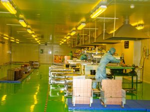 Soldermask printing: Apply solder ink on copper surfaces that do not require welding to prevent short circuits during welding. The LHD PCB factory supports various solder mask colors, such as green, matte green, white, matte white, black, matte black, blue, red, yellow, gray, purple transparent colors, etc. Customers can provide color cards, and LHD Tech’s PE engineers will match the corresponding colors according to the customer’s color card.
-Silkscreen printing: Printing component identification, component location, and other information on PCB soldermask for easy assembly . LHD PCBs normally use character printers for fast prototyping samples and screen printing for bulk production.
10
Milling and cutting the board to unit PCB
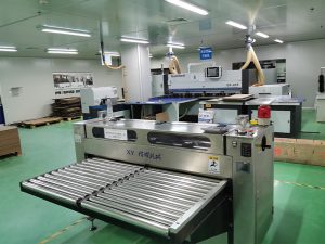
-Milling: Cutting or stamping production panels into the dimensions and shapes that customers need to deliver. The connection methods between unit PCBs include V-cut, bridge, mouse bite, etc. At the same time, our company can also produce punching. For some PCBs with low tolerance requirements and big qty, punching can be used to reduce costs.
-Silkscreen printing: Printing component identification, component location, and other information on PCB solder mask for easy assembly. LHD PCBs normally use character printers for fast prototyping samples and screen printing for bulk production.
11
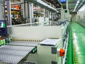
E-testing and FQC
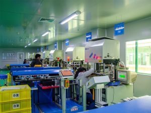
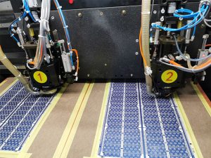
-E-testing: Use a flying probe testing machine or a fixture testing machine to check if the PCB is correct and if there are any short circuits or open circuits. LHD PCB supports flying probe testing and fixture testing, and all PCBs produced by LHD Tech undergo 100% E-testing to ensure that all PCBs are good.
-FQC and AVI testing machine: Check the overall appearance of the PCB, pad layout, and wiring for defects.
12
Packaging and Shipment
 -Packaging: LHD PCB will vacuum package all PCBs to ensure that the boards are not damp for a certain period of time. Heavy foam will be added around all boxes to ensure that the PCBs are not damaged during transportation.
-Shipment: The finished PCB will be sent to the customer through various transportation methods. Our company supports various delivery terms, such as FOB, CIF, DAP, DDP, DDU, etc; At the same time, I can also ship to customers through various express channels, such as DHL, USP, FedEx, TNT, etc. If customers need sea or land transportation (China Europe railway transportation), they can also support it.
