

Common Techniques Involved in the PCB Routing Process
The intricate pathways etched onto a PCB, known as traces, are the vital lifelines that connect electronic components and allow signals to flow. This meticulous process of defining these pathways is called PCB routing. Mastering PCB routing techniques is essential for ensuring the functionality, performance, and overall success of your printed circuit board design.
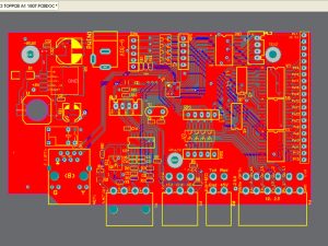
-300x225.jpg) The PCB Routing Process
The PCB Routing Process
PCB routing, while seemingly a straightforward act of drawing lines, is a well-defined process that requires meticulous planning and execution. Here’s a breakdown of the key steps involved in the PCB routing process:
- Netlist Import and Component Placement: The first step involves importing a netlist, a file that defines the electrical connections between components. Using specialized design software, components are then strategically placed on the PCB layout, considering factors like signal flow, heat dissipation, and manufacturability.
- Routing Strategy and Rule Definition: With components in place, the routing strategy comes into play. This involves defining design rules such as trace width, spacing, and layer assignments. LHD TECH’s one-stop service includes expert consultation to ensure your routing strategy aligns with your project’s specific needs.
- Manual Routing and Design Rule Checks: The heart of the process involves manually routing traces between components while adhering to the defined design rules. Sophisticated design software assists with this task, providing tools for trace placement, via insertion, and real-time design rule checks to identify potential errors.
- Design for Manufacturability (DFM) Review: Once routing is complete, a Design for Manufacturability (DFM) review is crucial. This ensures the PCB layout can be effectively manufactured within industry tolerances. Our team at LHD TECH offers comprehensive DFM reviews to identify and address any potential manufacturability concerns before production begins.
- Gerber File Generation and Fabrication: The final stage involves generating Gerber files, the industry-standard format for PCB manufacturing. These files precisely define the copper traces, solder pads, and other features on the PCB, allowing us to fabricate your board to your exact specifications.
 PCB Routing Techniques: The Art of Signal Flow
Within the PCB routing process, mastering specific routing techniques is essential for optimizing performance and ensuring signal integrity. Here are a few common techniques employed by PCB routing specialists:
- Manhattan Routing: This technique prioritizes straight lines and 90-degree turns, resulting in a clean and organized layout. It’s ideal for simpler PCBs with minimal routing complexity.
- Controlled Impedance Routing: For high-speed circuits, maintaining a consistent impedance (resistance to electrical current flow) is critical. Controlled impedance routing techniques ensure signal integrity by carefully managing trace width and spacing.
- Differential Pair Routing: In high-speed differential signaling applications, maintaining equal lengths and proximity between signal pairs is essential. Differential pair routing techniques achieve this by meticulously routing these pairs together throughout the PCB layout.
LHD TECH: Expert PCB Routing Solutions
At LHD Tech, we understand the significance of skilled and experienced PCB routing. Our team of experts leverages advanced design software and proven techniques to ensure your PCB layout functions flawlessly. Whether you require high-speed signal routing or a space-optimized design, we have the expertise to deliver exceptional results.
PCB routing is a fundamental yet intricate process that plays a critical role in the success of your PCB design. By understanding the PCB routing process, familiarizing yourself with common techniques, and partnering with us, you can ensure your electronic project operates at its peak potential.


