

PCB Design
Home > PCB Design
Layout Optimization
Using diagonal lines will free up some space, which can also be used for other shorter tracks. The main reason is to modify the VCC track here. One audio track (the highest VCC path) is torn apart and routed again.
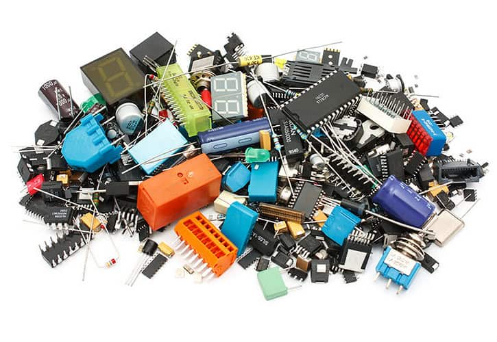
SMD means "Surface Mount Device".
SMD components can be placed by machine SMD components are smaller Before placing the parts, use the stencil to screen print the solder Soldering is carried out in a reflow oven or gas phase oven
Fiducials
The SMD assembly machine uses the camera reference circuit board. The benchmark lightweight structure is easy to find. Larger fine-pitch ICs should also have two reference points near them.
Gerber Files
Gerber files contain drawing commands for standard plotters.These photo plotters can "draw" the film used in PCB production.There is one film for each layer, so there is one Gerber file for each layer. The preferred Gerber format is RS-274X.
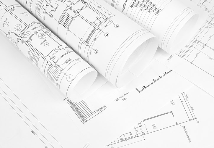
Schematic Diagram
The circuit design drawn in the CAD program is not only the lines on the paper, but also the circuit connection data drawn. When drawn correctly, it contains the parts and their interconnections.
It is important to connect the ends of the pins with “wires”, otherwise, they may appear to be connected but not connected. Therefore, it is recommended that the grid and snap to grid always remain open.

Provide your idea and requirements

Brainstorming with each other
Design Schematic Diagram
Component Procurement

Layout and Simulation

Prototyping and Sample Testing
A good layout starts with a good components library
Before using tools to draw schematics, you need to have a library containing component symbols and packages and use them in your project. Many people try to find a library on the Internet and even ask for a library on a forum. It must be time-consuming, and you never know what you will get. Usually, the symbols of these libraries are not the largest, take up space, and may not even be approved. I suggest you make your library.
Spend a lot of time thinking about schematic symbols. It may be good to use the same symbols as in the datasheet. Maybe not. It is recommended to group the pins, and these pins are usually connected (via wires or other components) or used together, such as data bus pins. It is not good to create a symbol similar to a physical IC pin. The “direction” of the pins should be correct. It can be in, out, passive, power, etc. This may help reveal the fault.
The placement is very important
After drawing the schematic, you need to create a circuit board file. This is usually easy. Just click an icon to enter the PCB editor.
Firstly, these parts were placed outside the PCB of standard size (for example 100mm x 160mm). These placements usually don’t make any sense. The thin lines connecting the pads are called tracks. Their connections created follow the schematics. The step of layout is to create needed copper traces on the copper pattern layers. But first, the parts must be placed in a meaningful way.
The time spent in a decent location is usually not wasted. Several standards must be met and sometimes contradict each other.
Most time the connectors should have to be put on one side of the board. Also, the electrolytic capacitors need far away from the heatsink, the heatsinked will dry out their electrolyte and they can not work. The track needs as short as possible, etc.
