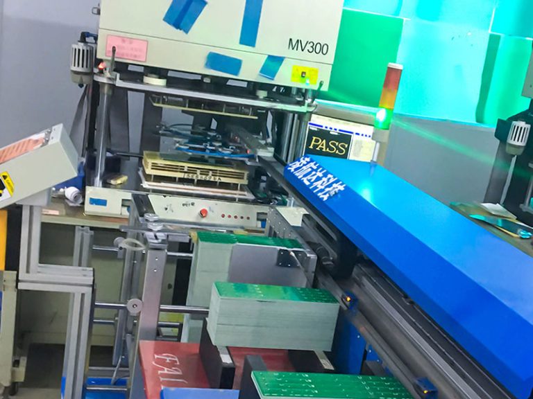
Surface completions for PCB vacillate in unwavering quality, time span of usability, evenness, cost, and get together strategies. All completions have their own advantages; be that as it may, the procedure, item, and/or last use figure out which surface completion works best for use with a particular application. The creator, end-client or constructing agent needs to work with the PCB producer to pick the right completion for the item plan.
Hot Air Solder Leveling (HASL)
Hot Air Solder Leveling (HASL), a 63/37 tin lead patch, has filled in as the business standard since the beginning of the circuit board. HASL is the most loved in light of the fact that “Nothing Solders like Solder.” In circumstances where you have no worry about lead, HASL demonstrates financially savvy just as a dependable completion for the creation of PCB of standard innovation. This completion does, in any case, further weight on high layer circuit sheets, bringing about incapable long haul use. The additional pressure, short time span of usability, and uneven binding stature on thick SMT or BGA cushions settle on HASL an awful decision for wire holding or chip innovation. New advancements, more tightly plan standards and natural issues are beginning to make HASL outdated. There are many without lead composites that can supplant the 63/37 tin lead weld procedure to make the board ROHS/Lead Free.
LeadFree Hot Air Solver Level (LF HASL) is the ROHS agreeable form of HASL. It is connected in the equivalent yet it is an alternate piece of the Solder. To consent to Lead-Free, the lead is expelled and supplanted by Gold, Nickel or different metals relying upon your PCB maker – along these lines the thickness changes anyplace between 1 and 15 mm.
Immersion Silver
Immersion Silver is a basic procedure. The silver replaces the copper amid the submersion procedure. It is rapidly picking up acknowledgment as a sans lead surface completion as a result of its lower cost (Compared to ENIG), uniform thickness and the ability to withstand the without lead get together temperatures. Submersion silver has a time span of usability of one year. Immersion silver has a controlled thickness of 6-10 small scale inches and remains cost proficient, good with most of gathering forms.
Electrodes Nickel/Immersion Gold (ENIG)
In the past clients perceived ENIG as the best level (fine pitch) surface and without lead decision on the planet. This surface completion holds a few favorable circumstances, including outstanding time span of usability and long haul understanding as well as information of the item. Nickel thickness for the most part estimates 75 micro inches, contrasted with 1-8 micro inch for gold.
Immersion Tin
Immersion Tin process, progressively prominent previously, offers a reliable level surface around 20-40 smaller scale inches thick. It binds well and remains cost effective. In any case, the completed PCB have a restricted time frame of realistic usability requiring you use them inside three to a half year. PCB manufacturing plants worldwide have this procedure set up. It is additionally ideal for Lead Free get together.
Organic surface preservative(OSP)
OSP started during the 1970s and give a thickness so fine you nearly can’t quantify it. The primary equations offered a restricted time span of usability of three to a half year and withstood just a single or two warmth cycles, yet today the most up to date OSP recipes offer significantly more in view of their development for lead free get together and give time frame of realistic usability a year just as the capacity to deal with various warmth cycles.
Electrodes Nickel – Electrodes Palladium – Immersion Gold (ENEPIG)
ENEPIG Is considered by numerous individuals call it – the “All inclusive” wrap up. Is a mix of three metals-nickel, palladium and gold. It is viewed as the best surface completion for Lead-Free get together and wire holding. Due to the mix of the three metals, it has the best galvanic opposition. The palladium isolates the gold from the Nickel to counteract clamor voltage and stop consumption. Additionally, as a result of the falling cost of Palladium, it has turned out to be all around sensibly estimated.
Plating Gold/Hard Gold
Hard Electrolytic Gold consists of a layer of gold-plated over a barrier coat of nickel. Hard gold is extremely durable, and is most commonly applied to high-wear areas such as edge connector fingers and keypads. Unlike ENIG, its thickness can vary by controlling the duration of the plating cycle, although the typical minimum values for fingers are 30 μin gold over 100 μin nickel for Class 1 and Class 2, 50 μin gold over 100 μin nickel for Class 3.
Hard gold is not generally applied to solder able areas, because of its high cost and its relatively poor solder ability. The maximum thickness that IPC considers to be solderable is 17.8 μin, so if this type of gold must be used on surfaces to be soldered, the recommended nominal thickness should be about 5-10 μin.
-768x513.jpg)
-768x576.jpg)