What are high-density interconnect (HDI) boards?
HDI is the English abbreviation of high-density interconnect, that is high-density interconnect (HDI) boards, which is a circuit board with relatively high circuit distribution density using micro-blind and buried via technology.
High-density interconnect (HDI) boards are used more and more for some complex designs to reduce the space and thickness, communication industry and military aerospace products have too many boards that use high-density interconnect (HDI) technical to design, this will save too much money and time for their projects. Also, the most popular products such as IOT and smart wearable products all use high-density interconnect (HDI) boards, High-density interconnects (HDI) boards can make the PCB smaller to save space, the finish products will more cheap and portable.
The High-density interconnect (HDI) boards have inner layer and outer layers, and then use lasing drilling and fill copper process in the hole to realize the internal connection of each layer of lines. Generally, the build-up method is used for manufacturing. Ordinary High-density interconnects (HDI) boards are basically layered once, and high-end HDI uses two or more layers of layering technology, as well as advanced PCB technologies such as laser direct drilling, electroplating hole filling, and stacking holes.
LHD can produce high-density interconnect (HDI) boards with different stack up
LHD PCB normally use three types of stack up for high-density interconnect (HDI) boards, they will build up with high-density packages:
- One-step high-density interconnect (HDI) board with only through holes and blind vias.
- One-step high-density interconnect (HDI) board with PTH holes, Blind vias, and Buried Vias.
- Two-step high-density interconnect (HDI) board Buildup with many microvias in more than two layers.
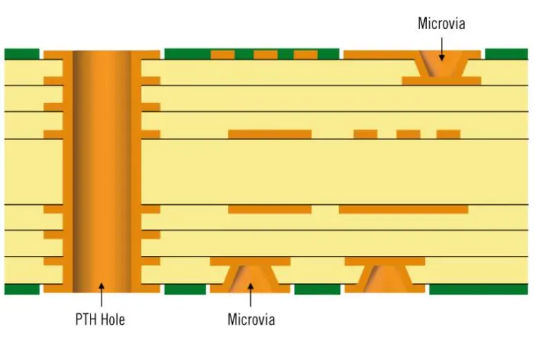
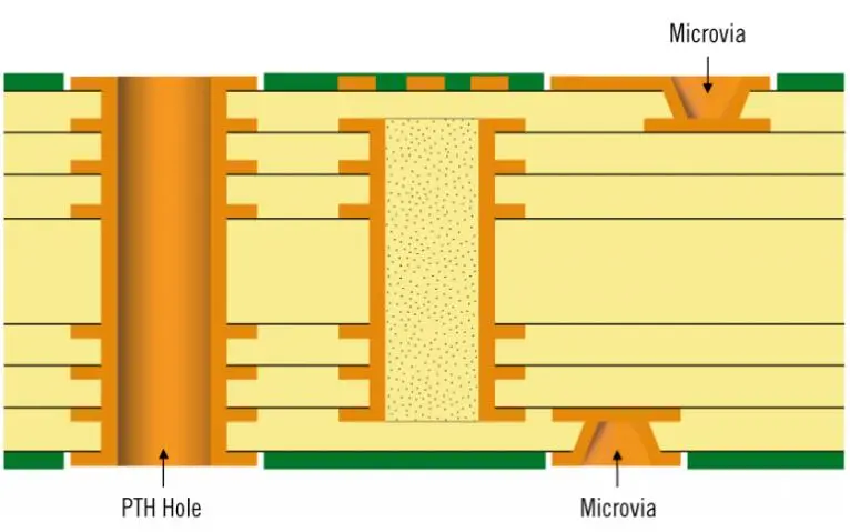
Stackup for high-density interconnect (HDI) boards
Following the IPC-2315 standard from the Institute of Printed Circuits (IPC), PCB manufacturers may use high-density interconnect (HDI) PCB stack up of types I, II, III, IV, V, or Vi. But the type IV, type V, and type VI are very expensive than normal cases.
The standard differentiates high-density interconnect (HDI) stack up with the use of vias, micro vias, blind vias, and buried vias, along with PTH holes, although the use of the lasing drilling is not strictly necessary for flex PCBs.
Type I stack up for High-density interconnect (HDI) board
High-density interconnects (HDI) PCBs of Type I stack up have a structure of a laminated core with at least one layer of micro vias on one or both of its sides. Type I High-density interconnect (HDI) may use PTH vias and blind vias, but without buried vias.
But there are 2 factors that limit the counts of layers in the laminated core of Type I HDI PCBs:
- The max aspect ratio must be less than 10 to maintain reasonable reliability.
- The thin FR-4 core may delaminate when used at high temperatures to do lead-free soldering.
So the Type I HDI stack up will not be significantly better than the normal large dense boards with multiple BGAs, because the PTH via pads will need to grow larger for higher layer counts. And the use of a single micro via layer does not offer appreciable benefits with the introduction of special features such as smaller diameter vias and thinner traces.
Type II stack up for High-density interconnect (HDI) board
High-density interconnects (HDI) board Type III also uses micro-vias, blind vias, and buried vias, at least on two layers of microvias on one or both sides. LHD PCB and the other manufacturers can stagger microvias from other microvias, and stack them or stagger them relative to buried vias.
Though the High-density interconnect (HDI) board Type II stack up is significantly better than Type I for bigger dense boards using multiple fine pitch components, it has the same limitations as that of Type I in the context of the limitations on the counts of laminated core layers.
Because Type II High-density interconnects (HDI) PCBs can have micro-vias only on their outer layers, it is not very effective when there is only a single buildup layer for trace routing.
Type III stack up for High-density interconnect (HDI) board
High-density interconnects (HDI) Type III structure construction also uses micro-vias, blind vias, and buried vias, with at least two layers of micro vias on one or both sides. LHD PCB and the other manufacturers may stagger micro vias from other micro-vias, and stack them or stagger them relative to buried vias.</p
Type III High-density interconnects (HDI) PCBs provide the best build-up for large dense multilayer PCBs using multiple large fine pitch BGAs, though they have the same limitations on the number of layers as faced by Type I and II when they use PTH holes and thin FR-4 cores.
Using micro vias in the inner layers of Type III High-density interconnect (HDI) PCBs allows the outer layers to be used for ground and/or power planes, leaving an adequate number of layers for signal routing. In addition, designers can obtain greater wiring density by stacking vias, but at a higher cost.
Summary
Designers can use different stack up to do the High-density interconnect (HDI) board, they can choose them based on the application and available budget. And Type III is the best and the most widely used in the PCB world. LHD PCB can provide both Types I, II, and III for you, all base on your design and requirements for the High-density interconnect (HDI) board. Please feel free to drop your questions to us, LHD PCB has a professional team to help you.
-768x576.jpg)