Multi-layer vs. Double-sided PCB
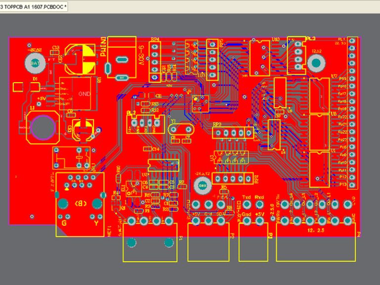
Multi-layer PCB (MLB) process
The simplest Multi-layer PCB starts with a double-sided core. This thin, inner-layer material has copper on both sides. The copper surface is prepped with a photosensitive material that can be exposed by the application of UV light, and the light is then applied either through a photo mask or with a raster scan laser (called, Laser Direct Image). The exposed areas of the photo mask are used to mask the copper traces n’ spaces from an etching process (usually cupric chloride in a spray application). The exposed copper of the core is etched away, leaving the core with the trace n’ space pattern of the inner layer. This is only a print-and-etch process. There are no holes in the core at this stage.
The etched inner layers are further processed chemically and then (in a layup process) sandwiched between pre preg (glass Matt that is saturated with a B-stage epoxy), placed in a heated laminating press and cured into a single piece. Thin copper sheets (typically 1 ounce or 1.4 mils thick) are laminated with the core and pre preg such that the resulting brick resembles an unprocessed sheet of double-sided laminate.
Double-sided PCB (DSB) process
The final process stage of all PCB is the double side process. This is true for even the most complex, multi-layer PCB. At this stage, there is a core of fiberglass (with or without inner-layers) covered by a thin layer of copper on both sides.
The double side brick is then:
Drilled
- Chemically processed (to prepare the drilled hole for adhesion of the thru-hole plating)
- Thru-hole plated (electrolysis copper that is very thin)
- Photo imaged (to transfer the outer layer pattern of traces n’ spaces)
- Electroplated (to build the final thickness of copper in the thru-holes)
- Etched (to remove the base layer of copper)
- Solder-masked (to protect the copper that will not get a final surface finish)
- Given a final surface finish (HASL, ENIG, Immersion Silver, Tin, OSP, etc.)
- Routed to final dimension desired by the customer
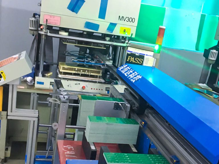
If you want to know more detail about the PCB manufacturing , welcome to visit PCB manufacturering Process(How Is A PCB Made in LHD tech
-768x513.jpg)
-768x576.jpg)