PCB vias and holes
In PCB manufacturing process, holes, also known as vias or vias, require square dimensions to connect various layers at different spots. Changes to leaded parts that need to be mounted on the PCB may necessitate holes. Furthermore, some fastening holes are required.
To electrically connect the layers of the board, the inner surfaces of the holes are usually coated with copper. A plating procedure was used to create these “plated through holes.” The layers of the board are frequently joined during this method.
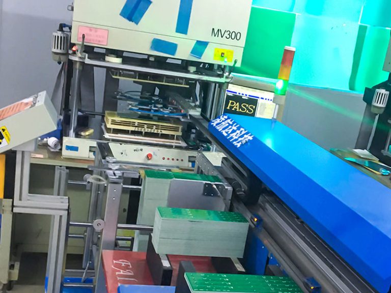
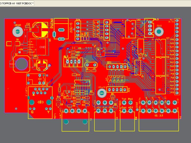
Drilling is then carried out using numerically controlled drilling equipment, with the data coming from the PCB CAD design package. It’s worth mentioning that minimizing the number of different hole sizes will help reduce PCB manufacturing costs.
When the inner layers of the board need forcing to be connected, it may be necessary for a few holes to only exist in the centre of the board. Before the PCB layers are secured together, these “blind vias” are trained within the necessary layers.
Solder resist and PCB solder plating
When soldering, a PCB it’s essential to keep the parts that don’t appear to be soldered shielded by a layer of solder resistance. This layer’s installation helps prevent unwanted solder short circuits on the PCB boards. Solder usually resist a compound layer that shields the board from solder and other impurities. The solder usually resists a deep inexperienced or red colour.
Exposed square measures of the board are usually “tinned” or plated with solder to alter the parts further, either led or SMT to solder to the board simply. Boards, or portions of boards, are sometimes gold-plated. If some copper fingers are used for edge connections, this could be useful. Because gold doesn’t tarnish and has good conductivity, it’s a good investment at a reasonable price.
Silk screening on PCBs
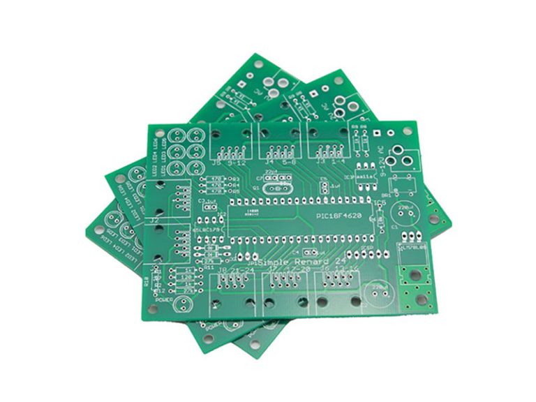
During the PCB-making process, it’s common to print text and place various tiny written indents. This will aid with identifying the board and the labelling of part positions to aid in fault-finding and other tasks. When the other manufacturing operations for the unoccupied board are completed, a silkscreen made by the PCB style package is used to feature the markings on the board.
Making a PCB as an example
Before committing to total production, it’s always a good idea to form an example as part of any development method. A similar situation exists with computer circuit boards, where a PCB example is often manufactured and tested in a factory before going into total production. In most cases, a PCB example must be factory-made fast due to the constant demand to complete the hardware design phase of the product development. Because the primary goal of the PCB example is to check the layout, it’s usually okay to utilize a different PCB manufacturing process because only a small number of the PCB example boards would be necessary. However, it’s always a good idea to stay as close to the ultimate PCB process as possible to ensure that few adjustments and new parts are included in the ultimate computer circuit board.
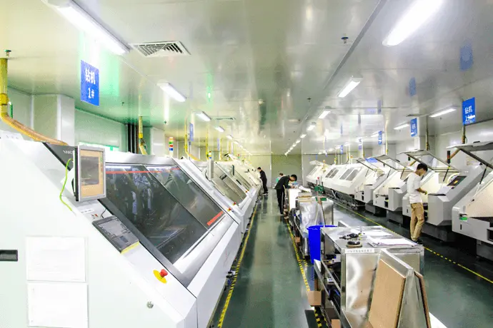
The PCB manufacturing process is essential for the natural philosophy manufacturing process. PCB manufacturing process uses a variety of modern technologies, which has resulted in significant improvements in the size of the parts and tracks employed and the board’s dependability.
-768x513.jpg)
-768x576.jpg)