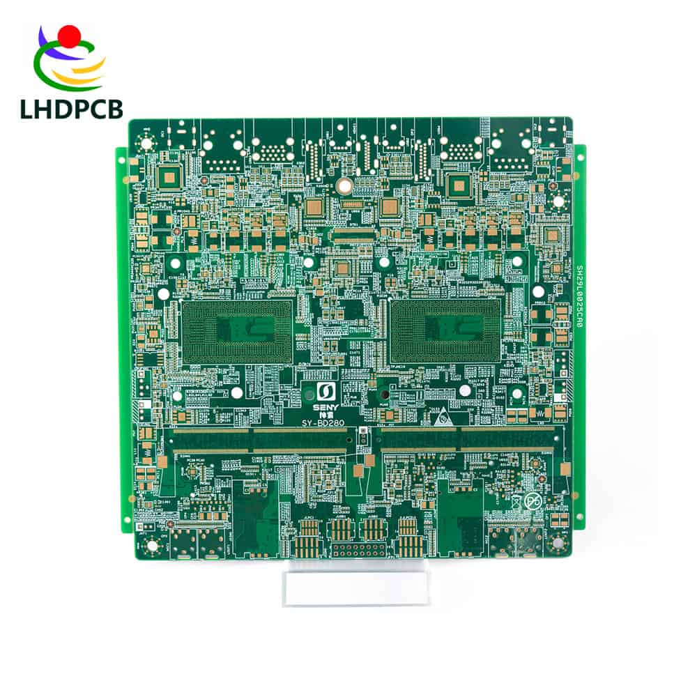
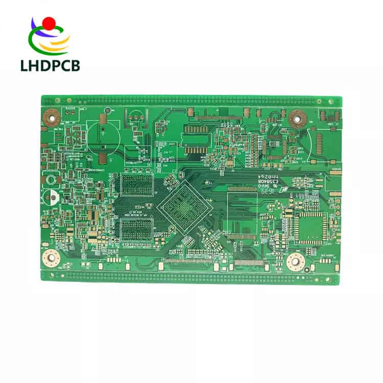
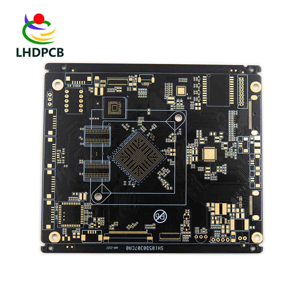
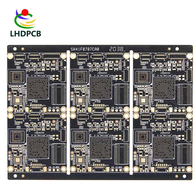
HDI PCB
What is HDI PCB?
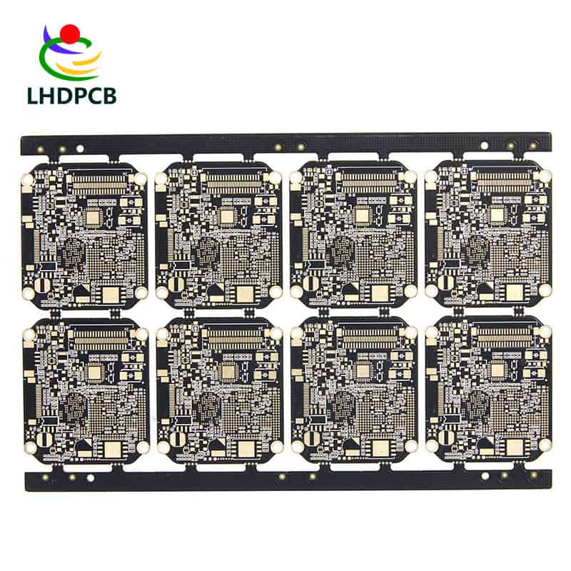
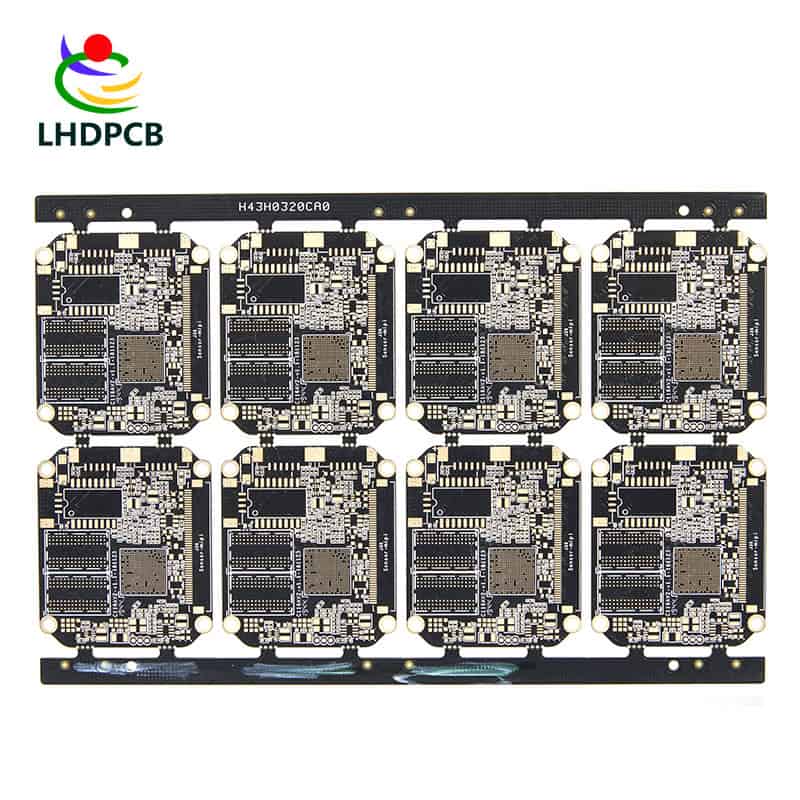
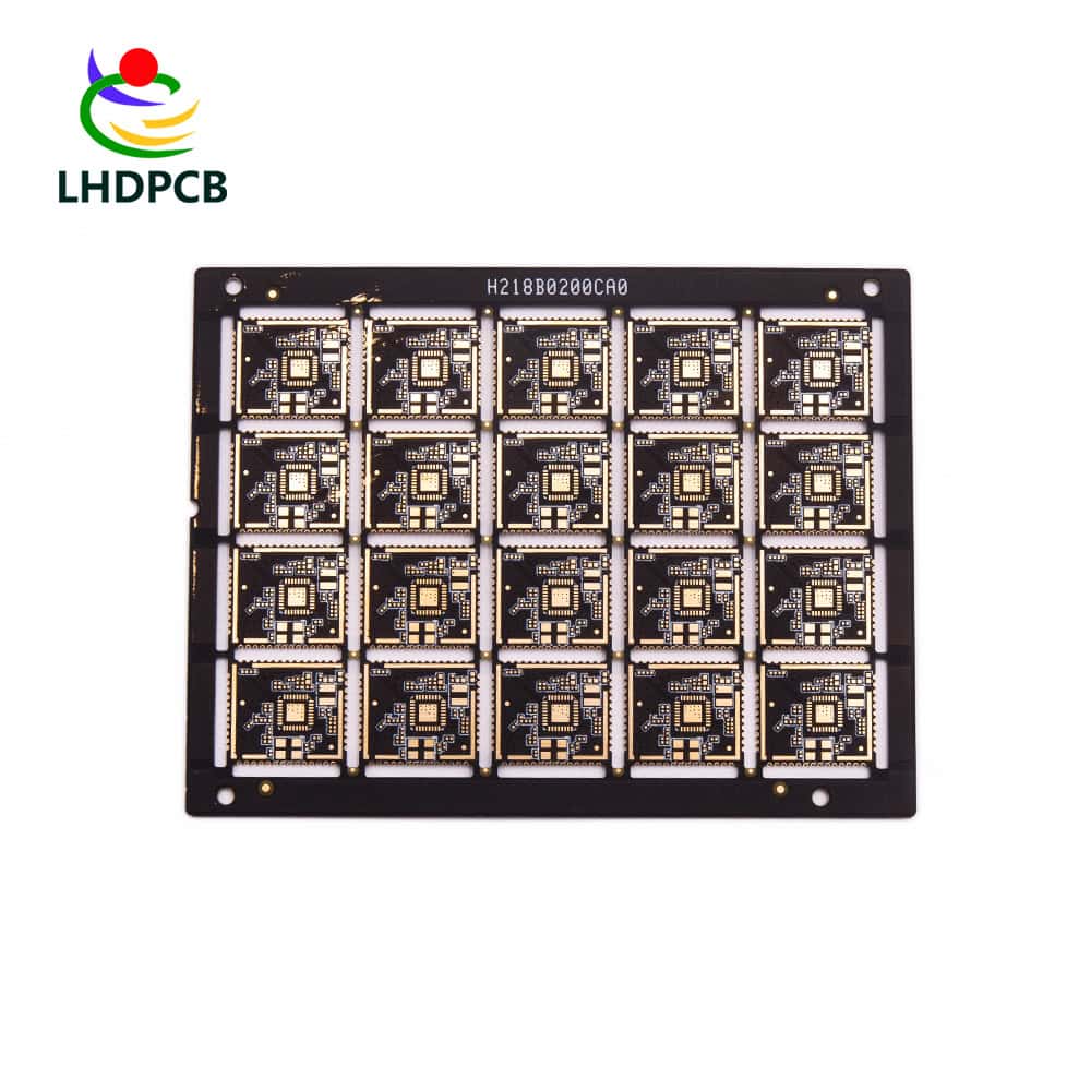
HDI is the abbreviation of High Density Interconnector (High Density Interconnector), is one of the production of printed circuit boards (technology), the use of blind hole technology, a circuit board with relatively high line distribution density.
Microhole ≤0.15mm, using fine line technology to connect components in very small packages. HDI technology enables end product design to be more miniaturized and meet higher standards of electronic product performance and efficiency. The HDI board has more laser drilling process than the traditional board. In the manufacture of HDI board, laser drilling, hole metallization and other processes need to be carried out to connect the internal lines of each layer. Moreover, the HDI board is manufactured by the lamination method, which requires multiple lamination, and the higher the technical grade of the board, the more advanced manufacturing technology needs to be adopted. In contrast, the traditional plate manufacturing process is relatively simple, usually using mechanical drilling, copper plating and other processes to achieve line connection.
In addition to the differences in manufacturing processes, HDI boards and traditional boards are also very different in structure and performance. HDI boards have a higher number of layers and a smaller line width and spacing, enabling higher signal transmission rates and less signal loss. At the same time, the HDI board also has better thermal stability and stronger corrosion resistance, and can adapt to more harsh working environments.
HDI board manufacturing needs to go through more and more complex processes and technologies, with higher technical content and better performance characteristics, is the electronics industry constantly pursue new technology and high quality products. In contrast, the manufacturing process of traditional boards is relatively simple, usually using mechanical drilling and electroplating copper and other processes to achieve line connection in addition to the differences in manufacturing process HDI boards and.
HDI board production process
Opening → inner graphic → inner etching → inner AOI→ brownization → pressing → Drilling buried holes → copper sinking in buried holes → Copper plating → Graphic plating → Pattern transfer → Etching → Laser drilling → mechanical drilling → Copper sinking → Electroplating → Pattern transfer →AOI→ welding resistance → Text → Surface treatment → Shape → Test inspection → packaging storage → Shipping
Why Choose Us?
High-Quality Standards
LHD TECH's stringent quality control: We adhere to strict quality control measures at every stage of production, from material selection to final inspection, to ensure that every PCB meets the highest industry standards.
Competitive Pricing
Cost-effective solutions: By optimizing our manufacturing processes and supply chain, we offer competitive pricing without compromising on quality.
Customization and Flexibility
We understand that every project is unique. Our ability to customize HDI PCBs to specific requirements allows us to meet the needs of a wide variety of applications and industries. Whether it's a small prototype run or a large production run, our facility can handle any size order with efficient turnaround times.
Proven Experience
With years of experience in the industry, we have a series of successful projects and satisfied customers who have demonstrated our capabilities and reliability, and we have been committed to solving challenging projects and providing innovative solutions that push the boundaries of HDI PCB technology.
Advantages of HDI printed circuit boards
Can reduce the cost of PCB
Increased line density
Advanced construction technology
High electrical performance and signal accuracy
The reliability is better
Can improve thermal properties
Can improve (RFI/EMI/ESD)
Increase design efficiency
Application Areas
HDI is widely used in mobile phones, digital cameras, laptop computers, automotive electronics and other digital products, among which mobile phones are the most widely used. HDI board is generally manufactured by Build-up method, the more times of stacking, the higher the technical grade of the board. The ordinary HDI board is basically 1 time stacking, and the high-level HDI uses 2 or more times stacking technology, while using advanced PCB technology such as stacking holes, electroplating holes, and laser direct drilling.
- Consumer Electronics
- Medical Devices
- Military and Aerospace
- Automotive Electronics
- Communication System
LHD Technology HDI PCB specifications
| Processing layers | 1-16 layers |
|---|---|
| Finished board thickness (thinnest - thickest) | 0.4mm~6.0mm |
| Minimum Hole Diameter | 6mil (0.15mm) |
| Minimum line width/spacing | 3-4 mil (0.076-0.10mm) |
| Maximum board size | Single and double layer 22″x 43″ (550 x 1100mm) Multilayer 22″x 25″ (550mm x 640mm) |
| Impedance control | ± 10% |
| Surface treatment process | oxidation resistant OSP, tin spraying, electric nickel/gold, chemical nickel/gold, lead-free tin spraying, gold finger, immersion silver, immersion tin, thick nickel/gold. |
| Processing materials | FR4, high TG (TG150, TG170), halogen-free sheet, high-frequency sheet, PTFE. |
Related Products