Heavy Copper PCB
What is Heavy Copper PCB
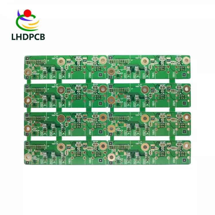
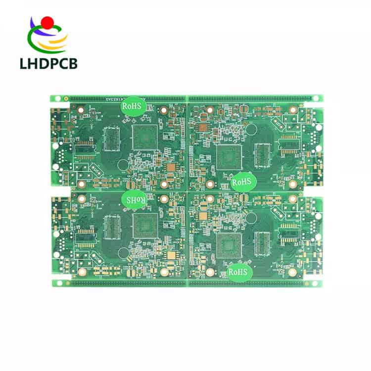
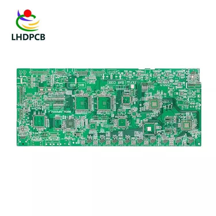
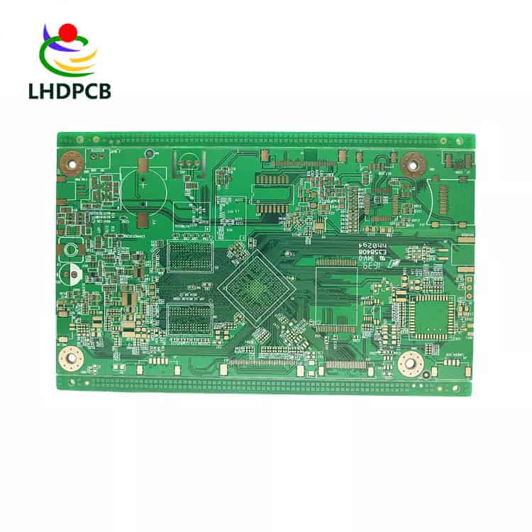
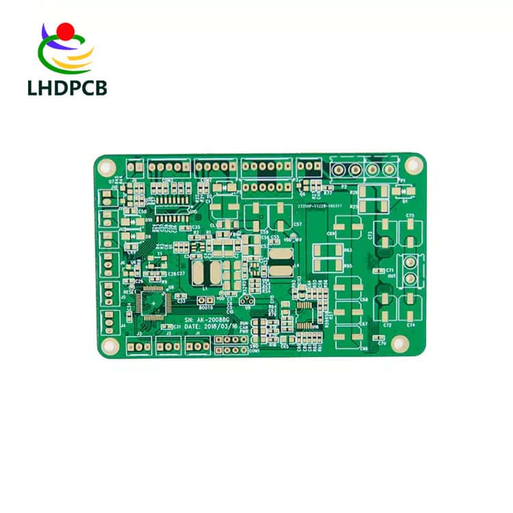
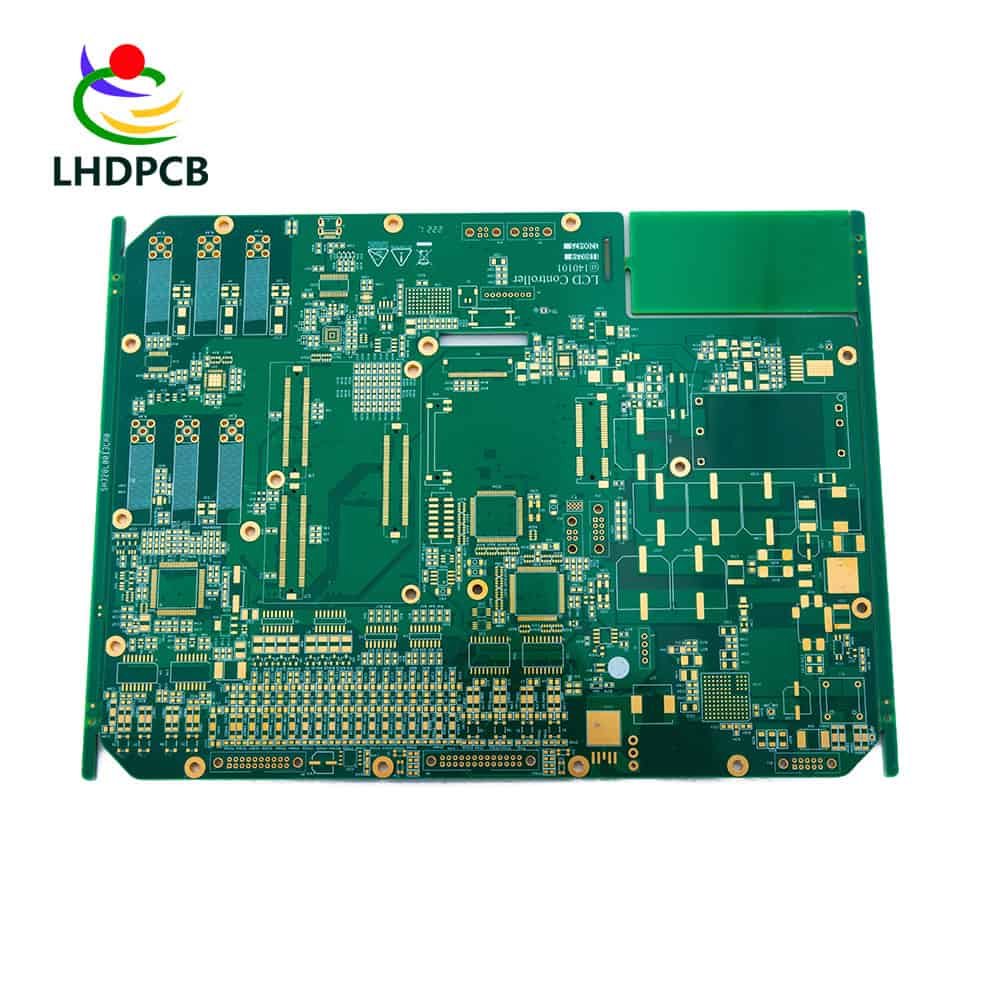
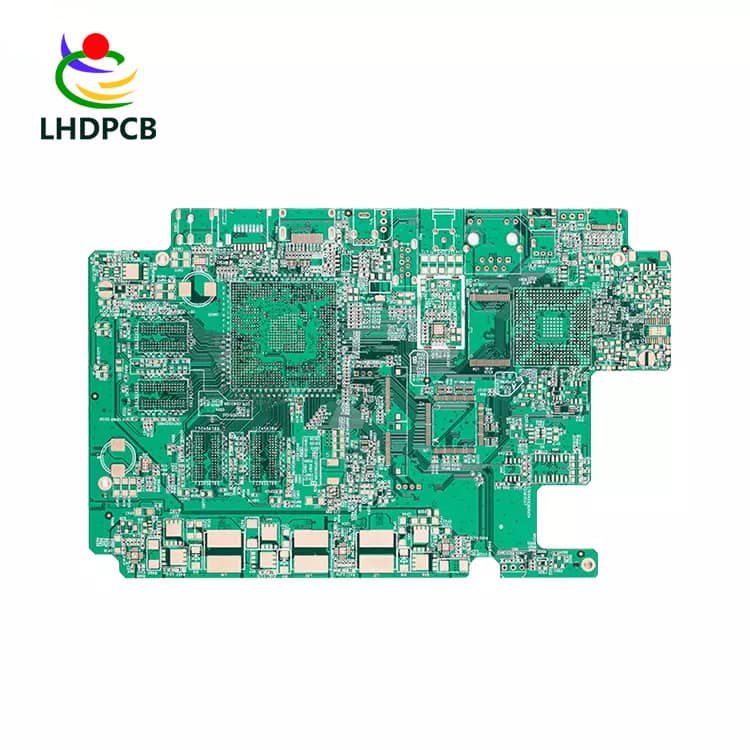
Thick copper printed circuit board is a printed circuit board made of thick copper foil. It uses materials (copper foil) and substrate sheet material, production process, application areas are different from conventional PCB, it is a special PCB. The thickness of the copper material used in such PCBS is in the range of 105-400 µm. In addition, thick copper printed circuit boards are able to maintain dissipation at high temperatures while providing a stronger connection. This thermal management feature ensures that thick copper PCBS are free from thermal stress. Common substrate: FR-4, CIM-3, CIM-1, 94HB, 94VO, polytetrachloroethylene, polyester, polyammonium imide.
The vast majority of thick copper printed circuit boards are high-current substrates, the main application field of high-current substrates is power modules and automotive electronic components, its main terminal electronic products in the field of portable electronic products, network supplies, base station equipment, automotive, industrial control, power modules.
Thick copper circuit board technology introduction
Preparation and electroplating before plating
The main purpose of thickening copper plating is to ensure that there is enough thick copper coating in the hole to ensure that the resistance value is within the range of the process requirements. As an insert, it is fixed in position and ensures connection strength; As a surface-packaged device, some holes only act as a through hole, playing a role in conducting electricity on both sides.
The vast majority of thick copper printed circuit boards are high-current substrates, the main application field of high-current substrates is power modules and automotive electronic components, its main terminal electronic products in the field of portable electronic products, network supplies, base station equipment, automotive, industrial control, power modules.
Why Choose Us?
Expertise
LHD has the professional team and experience to manufacture thick copper PCB.
Fast Delivery
We have efficient work processes and fully automatic production equipment.
Customization
We provide custom design and production services according to customers' specific requirements.
Quality Assurance
Strict quality control processes ensure the reliability and durability of our products.
Technical Support
Comprehensive technical support and optimization suggestions to ensure optimal product performance.
Copper Plating Process
In the process of thickening copper plating, the process parameters must be monitored frequently, which often causes unnecessary losses due to subjective and objective reasons. In order to do a good job of thick copper plating process, it is necessary to do the following aspects:
01.
According to the area value calculated by the computer, combined with the empirical constant accumulated in the actual production, increase a certain value;
02.
According to the calculated current value, in order to ensure the integrity of the coating in the hole, it is necessary to increase a certain value on the value of the original current, that is, the impulse current, and then return to the original value in a short time
03.
When the circuit board electroplating reaches 5 minutes, take out the substrate to observe whether the copper layer on the surface and the inner wall of the hole is complete, and the metal luster in all the holes is better;
04.
A certain distance must be maintained between the substrate and the substrate
05.
When the thickening copper plating reaches the required plating time, a certain amount of current should be maintained during the removal of the substrate to ensure that no blackening or darkening will occur on the surface of the subsequent substrate and in the hole.
Benefits of Heavy Copper PCB
High Current Carrying Capacity
Improved Heat Dissipation
Increased Mechanical Strength
Good stability
Heavy Copper PCB Application field
- Power Electronics
- Automotive Industry
- Renewable Energy
- Industrial Applications
- High-Performance Computing Hardware
- Military and Aerospace Applications
- Welding Equipment
LHD TECH Heavy Copper PCB Capabilities
| Processing layers | 1-50 layers |
|---|---|
| Finished board thickness (thinnest - thickest) | 0.4mm~6.0mm |
| Minimum Hole Diameter | 6mil (0.15mm) |
| Minimum line width/spacing | 3-4 mil (0.076-0.10mm) |
| Maximum board size | Single and double layer 22″x 43″ (550 x 1100mm) Multilayer 22″x 25″ (550mm x 640mm) |
| Impedance control | ± 10% |
| Surface treatment process | oxidation resistant OSP, tin spraying, electric nickel/gold, chemical nickel/gold, lead-free tin spraying, gold finger, immersion silver, immersion tin, thick nickel/gold. |
| Common substrate | FR-4, CEM-3, CEM-1,94HB, 94VO,Polytetrachloroethylene, polyester, polyammonium imide |
Related Products