Table of Contents
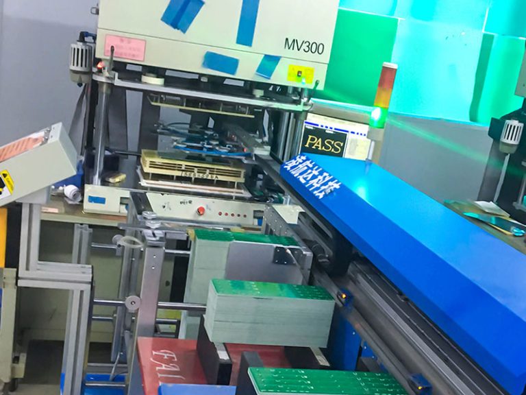
ToggleWith an increased demand for high-performing electronics, the necessity of dense, small and mid-sized PCBs has increased. Recently, circuit boards have been available in various designs and fit any specific requirement. Therefore, there have been multiple boards being developed by manufacturers, including 4 layer PCB manufacturing.
4 layers of PCB are multi-layered PCBs designed to meet various needs. This article will discuss their stack-up design, types, and advantages.
What is a 4-layer PCB?
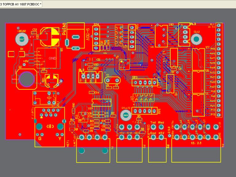
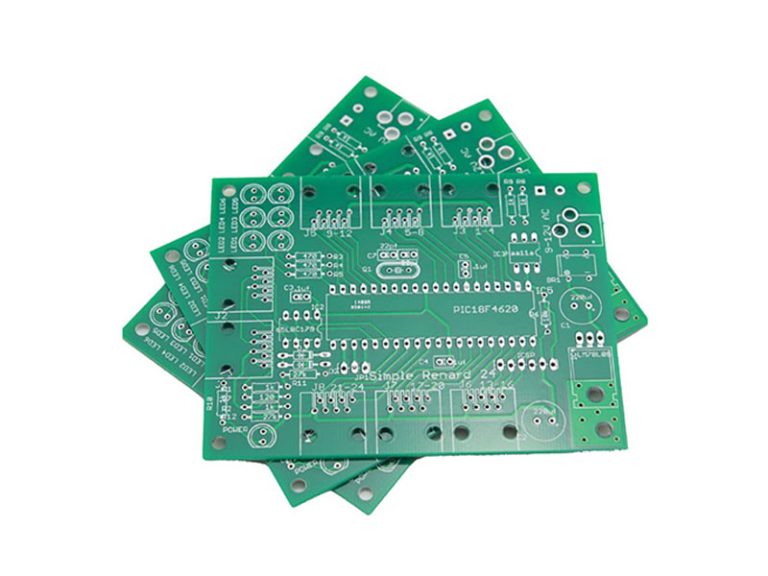
These are PCBs containing 4-conductive copper layers. The layers conduct electrical signals and are classified into outer and two internal layers.
The outer layers connect mounted components to the inner layer. On the other hand, the inner layer connects to the power planes and electrical signals. 4 layers PCB manufacturing is gaining popularity as the 4 layer PCB manufacturing simplifies signal transmission, component connections and also minimizes EMI emissions.
During 4 layer PCB manufacturing, two layers stack-up design is used. One inner layer conducts signals while the other behaves as a ground plane. But, both layers can work as ground planes bringing about parallel layering benefits.
The other alternatives use power and ground planes. However, manufacturers recommend designing the inner layer close to each other.
Advantages of 4 layer PCB manufacturing
- 4 layers PCB has two extra routing layers that facilitate complex device integration, signals, and board miniaturization.
- Essential to designers who design for PCB manufacturing. As we know, all commercial electronics must be certified. One common regulation requires PCB not to emit any radioactive component for a given period. 4 layer PCBs use power and ground protection to absorb radiated trace emissions.
- The arrangements of 4 layer PCBs make it easier for signal routing. That is because you can eliminate power and ground planes from routing layers and create more signal space.
The disadvantage of 4 layer PCB
- 4 layer PCB manufacturing tends to be expensive, making them a bit expensive. So, it’s not that desirable for simpler use cases.
- 4 layer PCBs conceal internal traces, complicating the circuit debugging process.
Applications of 4 layer PCB
Multiple PCB layers are used for a complex application. The various layers ensure more circuitry use for complex cases. So, if you want to use PCBs in equipment like smartphones, heart monitors, and computers, then multilayer PCBs are the best.
Here are the standard 4 layer board applications.
Medical equipment
There is increased demand for 4 layer PCB manufacturing in the medical industry because of its high functionality and miniaturized sizes. They are reliable in the medical industry from the treatment process to diagnosis. Testing machines, heart monitors, X-ray machines, and CT scans are common devices that use 4 layer boards.
Consumer electronics
Devices such as microwaves and smartphones, generally consumer electronics, have multilayer boards. This is due to the increased demand of multipurpose equipment which integrates well in our daily lives.
Other common application areas include;
Telecommunications: CPS, Satellite use, and signal broadcast.
Industrial: industrial controls.
Military and defense: high-speed military equipment.
Automotive: engine sensors, electric cars, devices control GPS, headlight switches, onboard machines.
Computer electronics: motherboards.
Aerospace: aerospace circuit board.
Choose LHD Technology for 4 layer PCB manufacturing.
Generally, 4 layer boards design minimizes design, facilitates complex routing, and increases EMI performance. That is why it’s essential in all industries. However, for the best 4 layer PCB, it’s essential to partner with experienced and reliable manufacturers. LHD Technology remains a leader in 4 layer PCB manufacturing and other multilayer boards. Get in touch!
-768x513.jpg)

-768x576.jpg)